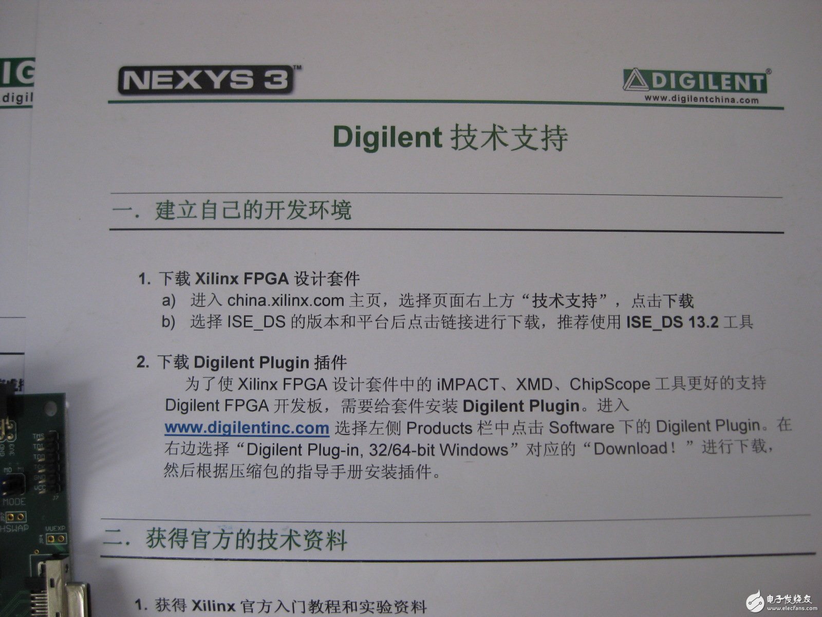
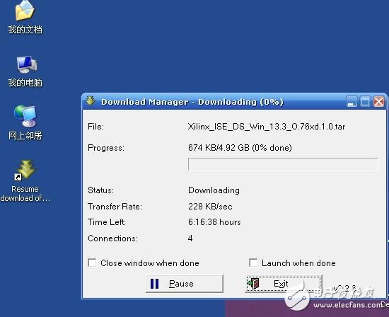
When I took over Nexys3, I thought I could provide a data CD. The result was disappointing. Except for a delicate circuit board in the electrostatic bag, there was only one USB cable and two loose pages for power supply and download. Fortunately, these two loose-leaf pages indicate the basic data request method. As shown in Figure 1, the first thing we need to do is to "build our own development environment". It can be said that "workers must first sharpen their tools when they want to do something good". Sharpening the knife does not mistake the woodworker.
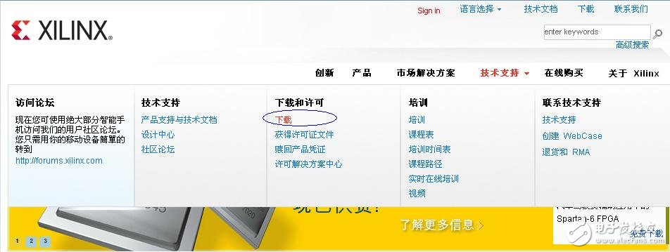
Go to the home page of china.xilinx.com, as shown in Figure 2, select "Technical Support" at the top right of the page, and click "Download".
After selecting the version and platform of ISE_DS and clicking the link to download, it is recommended to use the latest software version ISE_DS 13.3 tool. As shown in Figure 3, a friend using the Windows operating system can click the Full Installer for Windows to download.
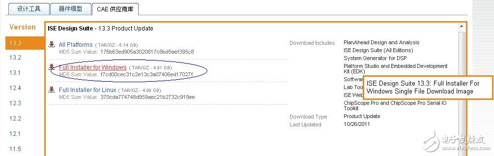
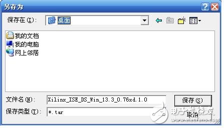
Figure 4 storage download software
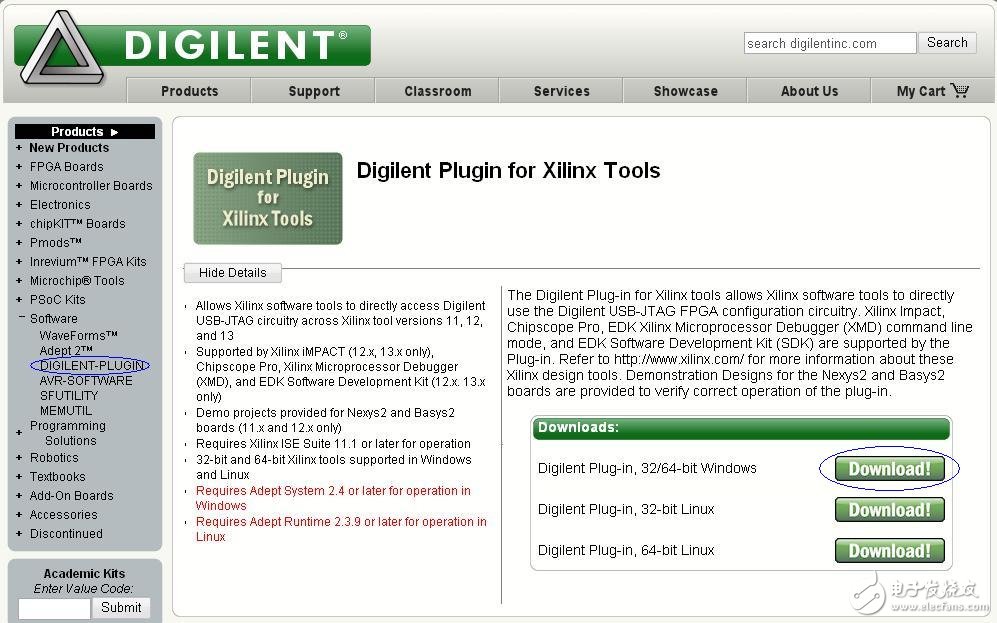
Download the Digilent Plugin plugin
In order for the iMPACT, XMD, and ChipScope tools in the Xilinx FPGA Design Suite to better support the Digilent FPGA development board, the Digilent Plugin needs to be installed on the kit. Go to the Products column on the left and click on the Digilent Plugin under Software. On the right, select "Download!" for "Digilent Plug-in, 32/64-bit Windows" to download, and then install the plug-in according to the instruction manual of the package. The Digilent Plugin plugin download page is shown in Figure 6.
Second, license application and software installation
Software Installation
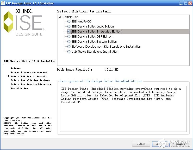
After the software download is complete, unzip Xilinx_ISE_DS_Win_13.3_O.76xd.1.0.rar and click on xsetup.exe to start the software installation. All the way to the next, until Select EdiTIon to Install, select ISE Design Suite: Embedded Editon, as shown in Figure 7.
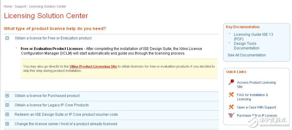
Click on "Technical Support à Licensing Solution Center" at the bottom right of the china.xilinx.com page, and click on "Obtain a license for Free or EvaluaTIon product" under "What type of product license help do you need?" on the new page. The drop-down information shown in Figure 9 pops up, then click on “Xilinx Product Licensing Site†to enter the license management page.
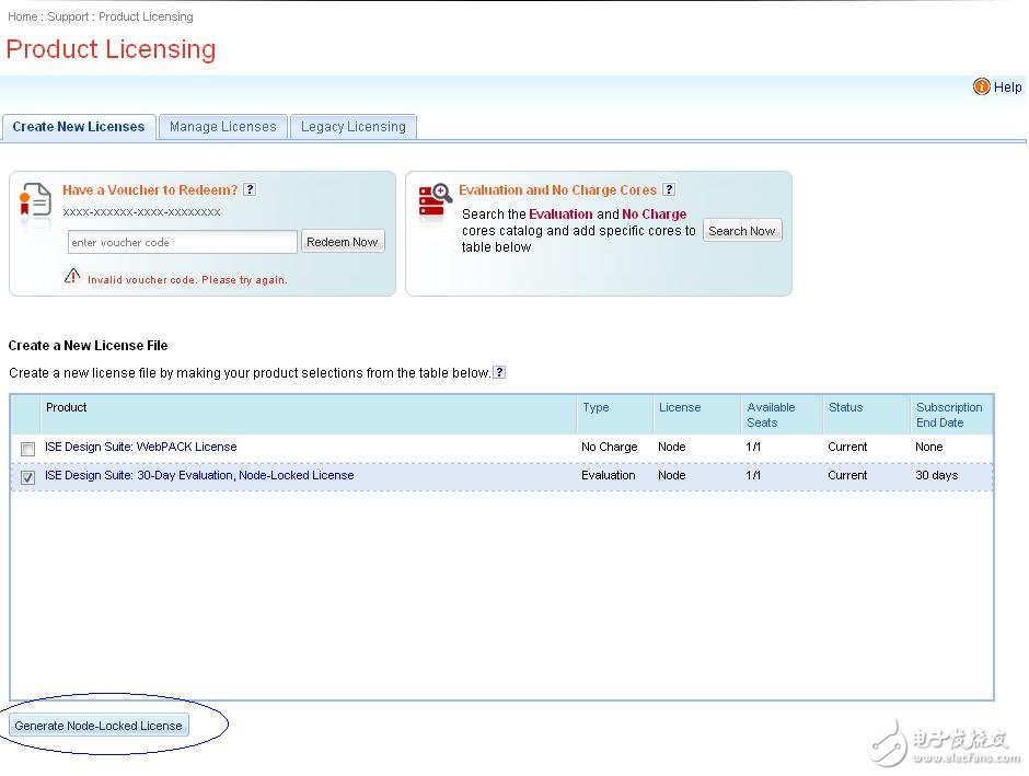
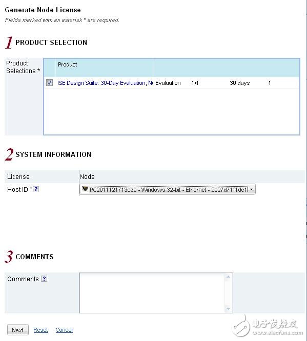
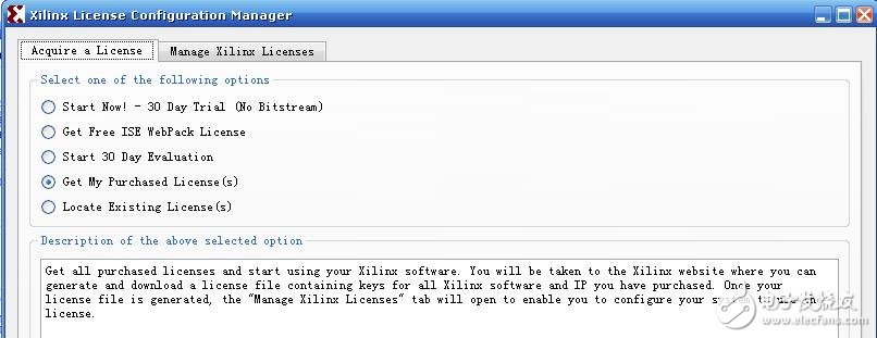
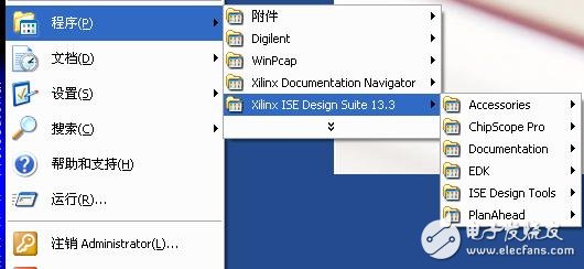
After completing the application and download of the license, we will continue to continue the "business" in the software installation process. In Figure 8, we select “Locate ExisTIng License(s)â€, then click “Copy License...†to locate the license for the new application. At this point, the dialog box "License installation was successful" pops up. Congratulations, the license installation is successful, and your development environment is ready for use. Well, as shown in Figure 12, Xilinx ISE Design Suite 13.3 has appeared in our system menu bar.
How does TFT work?
TFT is the abbreviation of "Thin Film Transistor", generally refers to thin film liquid crystal displays, but actually refers to thin film transistors (matrix)-can "actively" control each independent pixel on the screen, which is The origin of the so-called active matrix TFT (active matrix TFT). So how exactly is the image produced? The basic principle is very simple: the Display Screen is composed of many pixels that can emit light of any color, and the purpose can be achieved by controlling each pixel to display the corresponding color. In TFT LCD, backlight technology is generally used. In order to accurately control the color and brightness of each pixel, it is necessary to install a shutter-like switch after each pixel. When the "blinds" are opened, light can pass through, and " When the shutters are closed, light cannot pass through. Of course, technically, it is not as simple as the one just mentioned. LCD (Liquid Crystal Display) utilizes the characteristics of liquid crystals (liquid when heated, and crystallized into solid when cooled). Generally, liquid crystals have three forms:
Smectic liquid crystal similar to clay
Nematic liquid crystal resembling a fine matchstick
Cholestic liquid crystal
The liquid crystal display uses filaments, and when the external environment changes, its molecular structure will also change, and thus have different physical properties-it can achieve the purpose of letting light through or blocking light-which is just like the blinds just now.
Everyone knows the three primary colors, so each pixel on the display screen needs three similar basic components described above to control the three colors of red, green, and blue respectively.
The most commonly used one is twisted nematic TFT LCD (Twisted Nematic TFT LCD). Existing technologies vary greatly, and we will cover them in detail in the second part of this article.
There are grooves on the upper and lower layers. The grooves on the upper layer are arranged longitudinally and the grooves on the lower layer are arranged horizontally. When no voltage is applied to the liquid crystal in its natural state, the light emitted from the light emitting layer of the twisted nematic TFT Display working principle diagram of Figure 2a will be twisted by 90 degrees after passing through the interlayer, so that it can pass through the lower layer smoothly.
When a voltage is applied between the two layers, an electric field is generated. At this time, the liquid crystals are aligned vertically, so the light will not be twisted-the result is that the light cannot pass through the lower layer.
(2) TFT pixel structure: The color filter is divided into red, green, and blue according to the color, which are arranged on the glass substrate to form a group (dot pitch) corresponding to a pixel. Each monochromatic filter is called It is a sub-pixel. In other words, if a TFT display supports a maximum resolution of 1280×1024, then at least 1280×3×1024 sub-pixels and transistors are required. For a 15-inch TFT display (1024×768), then a pixel is about 0.0188 inches (equivalent to 0.30mm), for an 18.1-inch TFT display (1280×1024), it is 0.011 inches (equivalent to 0.28mm) .
As we all know, pixels are decisive for the display. The smaller each pixel is, the larger the maximum resolution that the display can achieve. However, due to the limitation of the physical characteristics of the transistor, the size of each pixel of the TFT at this stage is basically 0.0117 inches (0.297mm), so for a 15-inch display, the maximum resolution is only 1280×1024.
Tft Lcd Module,Lcd Liquid Crystal Display Module,Lcd Module,Lcd Screen Module
ESEN Optoelectronics Technology Co., Ltd, , https://www.esenlcd.com