12.2.7 PicoBlaze Instruction Memory Configuration Mode
The PicoBlaze microcontroller actually consists of two parts, the kernel KCPSM3 and the instruction memory ROM. To ensure that there are no writes during program operation, the WE side of the BRAM is grounded, as shown in Figure 12-18. Of course, in addition to this way, there are many other ways, which will be introduced one by one.
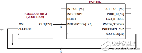
Figure 12-18 Standard configuration of the PicoBlaze microcontroller memory 1K&TImes;18
The application is compiled and integrated as part of the FPGA implementation and stored with the FPGA configuration file .bit. During the FPGA configuration process, the application is automatically loaded into BRAM, as shown in Figure 12-19.
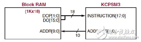
Figure 12-19 1K&TImes;18
Once the application is compiled, it can be synthesized without the FPGA and the BRAM data can be written via JTAG or UART, as shown in Figure 12-20.
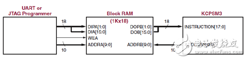
Figure 12-20 1K&TImes;18 (with UART or JTAG programming)
Both PicoBlaze share the same BRAM, and although they execute the same code, each microcontroller is executed separately, with its own independent IO, interrupt, and clock, as shown in Figure 12-21.
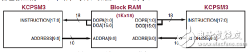
Figure 12-21 Two PicoBlaze shares 1K&TImes; 18
Divide one BRAM into two for use by two PicoBlaze. Note the connection of the address bit ADDRESS[9]. The configuration is shown in Figure 12-22.
Implementing PicoBlaze's instruction memory with distributed RAM is more suitable for applications with less instructions, because distributed RAM consumes LUT resources. If the RAM capacity is too large, it will affect the logic implementation. The configuration is shown in Figure 12-23.
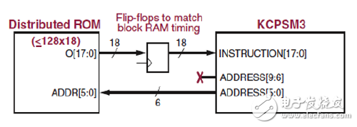
Figure 12-23 Using distributed RAM
Table 12-3 shows the consumption of SLICE for different depth ROMs.

52W Medical Adapter,52W Medical Outlet Adapter,52W Medical Ivd Adapter,52W Breast Pump Adapter
Shenzhen Longxc Power Supply Co., Ltd , https://www.longxcpower.com