1. introduction
GPS (GLOBLE POSITIONING SYSTEM) is a space intersection fixed-point navigation system that can be timed and ranged. It can provide global users with continuous, real-time and high-precision 3D position, 3D speed and practical information. GPS offers two services: Standard Positioning Service (SPS) and Precision Positioning Service (PPS).
The use of GPS technology for navigation and positioning of ground motor vehicles has a wide and important application value in both military and civilian applications. Nowadays, the automatic vehicle positioning and navigation (AVLN) system in various countries is diverse, but in terms of its system structure, it mainly includes three parts: in-vehicle system, communication system and central control management system.
The particularity of the in-vehicle system application environment has higher requirements on circuit performance, and the design of the RF circuit is the key to achieving high performance. If the RF circuit design is not good, the noise sensitivity and signal-to-noise ratio of the Receiver and other technical indicators will be greatly reduced, thus affecting the effect of the received signal.
Figure 1 shows the block diagram of the Automatic Vehicle Positioning and Navigation (AVLN) system. The design of the RF circuit in the GPS receiver front end will be the focus of this paper.
This article refers to the address: http://
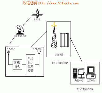
Figure 1: Block diagram of the automatic vehicle positioning and navigation (AVLN) system
2. Design requirements for RF receiver front end of GPS receiver
2.1 Basic Components of a GPS Receiver Most receivers have multiple channels, each of which tracks the transmitted signal from one satellite. Figure 2 shows a block diagram of a general multi-channel GPS receiver.
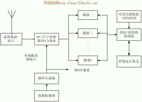
Figure 2: Basic block diagram of a general GPS receiver
The received RF CDMA satellite signal is first filtered with a passive bandpass filter to reduce out-of-band RF interference. Normally followed by a pre-release. The RF signal is then downconverted to an intermediate frequency (IF). In a typical modern receiver scheme, the IF signal is sampled and digitized using an A/D converter. The A/D sampling rate is typically 8 to 12 times the PRN base code rate. The minimum sampling rate is 2 times the band-stop bandwidth of the code to satisfy the Nyquist criterion. Oversampling reduces the receiver's sensitivity to A/D quantization noise, thus reducing the number of bits required in the A/D converter. The samples are sent to a digital signal processor. The DSP contains N parallel channels to simultaneously track carrier frequencies and codes from up to N satellites. A code and carrier tracking loop is included in each channel to perform code and carrier phase measurements, as well as demodulation of navigation message data.
2.2 Impact of radio frequency interference on tracking Since GPS receivers rely on external RF signals, they are susceptible to RF interference. RF interference can cause a reduction in navigation accuracy or a complete loss of receiver tracking. Table 1 summarizes the various types of RF interference. RF interference can be unintentional or intentional. Especially in the design of the car GPS receiver, it is necessary to consider the interference caused by the road surface condition and the mobility of the vehicle itself.
Table 1: Various RF interference types 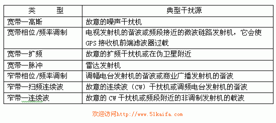
2.3 RF Front End Design Requirements The RF portion of the receiver includes all components from the antenna to the digital processor. This definition clearly indicates that the RF front end includes RF amplifiers, filters, downconverters, gain controls, and local signal generators. The RF front end also includes an antenna and a power supply line that supports RF operation. We know that the C/A code is a spread spectrum signal modulated at 1575.42 MHz at a code rate of 1.023 MHz. The satellite signal power reaching the antenna is about -130dBm, buried deep below the thermal noise electrons (-114dBm/MHz). Therefore, the RF front-end must amplify the signal above a certain level so that the signal can be utilized by the digital processor. Assuming that the level is 0 dBm/MHz, the total front-end gain is required to be no less than 110 dB.
The RF circuit must also downconvert the carrier 1575MHz to the digital processor's operating frequency range, the last stage of the intermediate frequency IF. The conversion from RF to IF can be achieved by one or several stages of downconversion, and the choice of IF and conversion stages is important for RF design. At present, the design of GPS receivers mostly uses two or more levels of conversion to change the RF to IF. This is because the gain stability is better at different frequency points, and the receiver's anti-interference ability can be improved due to more optimized filtering.
The above three parts - amplification, down conversion and filtering are the main parts of the receiver RF front-end design. The other two parts are automatic gain control (AGC) and local oscillator signal generator. The last part of the RF hardware is to generate the required local oscillator signal. Regardless of the number of downconversion stages, each stage requires a stable local oscillator signal source. This can be achieved by using a temperature-compensated crystal oscillator TCXO reference source and a PLL phase-locked voltage-controlled oscillator VCO, frequency multiplier, and frequency divider.
In addition, the GPS receiver noise figure is another issue that should be considered in the system performance indicators. The system works when the front-end noise figure of the civilian receiver is 4~6dB.
3. Design and Implementation of GPS Receiver for Vehicle System
3.1 The circuit of the GPS RF front end constitutes the RF part of the GPS receiver. Usually, the GPS RF signal received by the antenna is filtered and amplified by a low noise amplifier (LNA) and compared with the sine wave signal generated by the local oscillator. Mixing to form an intermediate frequency signal. The local oscillator of most GPS receivers uses a precision quartz crystal oscillator as the reference frequency synthesizer. In addition to the IF signal becoming lower at the carrier frequency, all modulated signal information of the RF signal is transferred to the IF signal. There must be an analog-to-digital (A/D) converter between the analog and digital parts of the GPS receiver. Some direct-sampling receivers are not facing the IF signal, but are directly A/D-sampling the RF signal. This is not advantageous in low-cost hybrid analog (A/D) chips. Direct sampling not only requires high-speed A/D converters, but more importantly, increases the processing power of the digital parts in the back. Figure 3 below shows the circuit design of the RF front-end of the GPS receiver used in the vehicle.
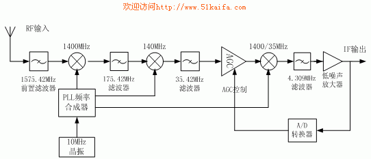
Figure 3: GPS receiver RF front end
3.2 Setting of RF Front End Technical Parameters The RF front end includes a 1400MHz PLL frequency synthesizer, a low noise amplifier, a three-stage mixer, and a 2-bit A/D converter. The front end receives the 1575.42MHz satellite signal and converts it to 4.309MHz IF through three-stage conversion. When the front end is used with a correlator, the latter provides a 5.714 MHz sampling clock, which converts the IF to a 1.405 MHz 2-bit digital signal for level output. The first stage and second stage mixers are balanced open collector inputs and outputs, requiring external DC offset and filtering. In the design, the 175.42MHz filter uses a simple two-stage LC-parametric tuned filter with a wide bandwidth, while the second stage uses a 1dB-band acoustic surface filter with a bandwidth of 1.9MHz. It has better out-of-band rejection and filtering the system. Performance plays a decisive role. In addition, the insertion loss of the two filters is also different, the former is lower and the latter is higher, and the performance of the two is complementary. The third stage output IF uses on-chip filtering. The gain quantization expression is:
-l 74dBm/Hz 19dBm+G1+G2+G3-21dB +63dB > -7dBm where:
1)-7dBm=typical level required for IF output during AGC operation 2)-174dBm/Hz=background noise level of RF input 3)19dB=sum of low noise amplifier gain and noise figure 4)-21dBm=175MHz, 35.42MHz filter insertion loss sum (175MHz filter insertion loss: 0~5 dB, 35.42MHz filter insertion loss: 14dB~16dB)
5) 63dB = sum of noise in the 2MHz bandwidth.
The above formula can obtain the requirements for the mixing gain of each stage, namely: G1+G2+G3>106dB
The G1, G2, G3 gain and AGC gain ranges are:
G1:11dB~25dB
G2: 22dB~33dB
G3: 106dB~G1-G2, the maximum is 75dB.
The AGC dynamic range is 60dB to meet the system's gain requirements.
4. Summary With the development of communication technology and semiconductor integration technology, GPS system has been widely used in aircraft navigation, ship access control, various vehicle positioning and command scheduling, base station or wireless local loop timing. In recent years, GPS systems have been widely used in various fields such as geodesy surveying, marine fishing, vehicle positioning monitoring, construction, and agriculture. Since the introduction of GPS positioning technology in China in the 1990s, after more than ten years of market cultivation, GPS positioning applications have entered the best opportunity for development. The application of GPS in the next decade will change the way we live and work.
Nh Fuse And Base,Low Voltage Fuse,Ceramic Fuse Base,Nt Fuse And Base
Tengqiang Electronics Co.Ltd , http://www.xingdaele.com