OLED (Organic Light-emitTIng Diodes), the Chinese name for organic light-emitting diodes, is a light-emitting diode based on organic semiconductor materials. OLED has many advantages such as all solid state, active illumination, high contrast, ultra-thin, low power consumption, no viewing angle limitation, fast response speed, wide operating temperature range, easy flexibility and large area, and low power consumption. At present, OLED has been applied in small-sized display fields such as mobile terminals, and the development potential in the field of large-size televisions and lighting has also been recognized by the industry. OLED has been recognized as one of the most promising display and lighting products of the 21st century.
OLED, it is officially on the stage of lighting from 2012, although it is only a small role, but there is no small substitute for LED.
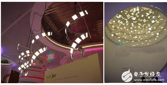
At the Frankfurt show in April, Philips unveiled the Lumiblade OLED GL350 panel for the latest OLED technology. Each GL 350 OLED panel measures approximately 155 square centimeters and has a brightness of 115 LM.
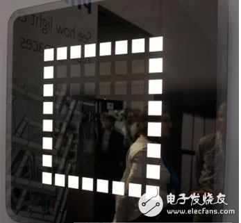
At the Las Vegas Lighting Show in the United States on May 8-11, 2012, Philips once again exhibited an OLED mirror product that automatically senses the proximity of the human body and automatically modulates the surrounding OLED light source. The group makes adjustments, and the middle becomes darker and becomes a mirror effect. Successfully integrated the concept of smart luminaires and OLEDs.
As the leading brand in the global lighting market, Philips, the meaning of betting OLED is very obvious.
However, OLED is used in the field of lighting, but the light effect is not a small test. In the display field, the brightness of the OLED reaches 100 to 300 cd/cm2, but in lighting applications, the brightness must be at least 1000 to 3000 cd/cm2. In the next few years, the speed of OLED and LED in the field of lighting will depend on the progress of OLED light efficiency.
Keyword 2: PSS
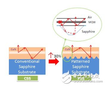
PSS (Patterned Sapphire Substrate), that is, a mask for dry etching is grown on a sapphire substrate, a mask is patterned by a standard photolithography process, sapphire is etched by ICP etching, and the mask is removed. A GaN material is then grown thereon to cause the longitudinal development of the GaN material to become lateral. On the one hand, the bit error density of the GaN epitaxial material can be effectively reduced, thereby reducing the non-radiative recombination of the active region, improving the internal quantum efficiency, reducing the reverse leakage current, and improving the lifetime of the LED; Light, which is multi-scattered by the GaN and sapphire substrate interface, changes the exit angle of the total reflected light, increasing the probability that the inverted LED light will exit from the sapphire substrate, thereby improving the light extraction efficiency.
Therefore, PSS has become the mainstream technology for brightness enhancement adopted by extension manufacturers for a time, and has rapidly become popular. By the second half of 2012, PSS has accounted for nearly 80% of the world's LED sapphire substrates.
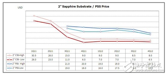
In the first half of the year, the price of sapphire substrate flats fell to a low point, and substrate manufacturers generally fell into losses. Because of the strong market demand, PSS has more than doubled the market price of flat film at one time, attracting the sapphire substrate factory to deploy more code, and hopes to break through the dilemma of revenue loss. However, as new capacity is gradually put into use, the speed at which PSS prices fall is also phenomenal.
Some large manufacturers have already considered adopting more advanced nPSS technology. The pitch of nPSS is less than 1um, and the brightness can be increased by 3% to 10% compared with PSS. The embossing is lower than the cost of etching by more than one dollar, and the stability and consistency are also good. I hope that the substrate factory that relies on PSS to save the tide will once again be disappointed, but who can guess the path of technological progress?
Keyword three: non-sapphire substrate
In addition to CREE's successful commercial SiC substrate, people have become accustomed to the substrate material is sapphire. However, in 2012, the non-sapphire substrate solution presented a threatening challenge to the status of sapphire substrates for the first time.
The most threatening challenge is undoubtedly from the silicon substrate. On January 12, 2012, Osram announced the successful extension of GaN on 150mm silicon wafers, and cut into 1mm2 at 350mA, the brightness can reach 140lm. The project is German federal education. And part of the "GaN on silicon" project funded by the research department.
Toshiba’s action is a step faster. In mid-December 2012, Toshiba, which was not involved in packaging, directly sold LEDs, and the chip used LEDs grown on 8-inch silicon substrates in cooperation with Bridgelux. chip. Toshiba has released four specifications for its current products, including a color temperature of 3000K, a color temperature of 4000K and two color temperature 5000K LED products. Among them, when the typical forward voltage is 2.9V, the 350mA driving color temperature is 5000K, and the color rendering index is 70. The model is TL1F1-NW0 LED, and the luminous efficiency reaches 110lm/W.
Image source: OSRAM
Image source: TOSHIBA
After years of hard work in the field of silicon substrates, Chinese manufacturer Jingneng Optoelectronics launched a luminous efficiency of more than 120lm/W silicon-based high-power LED chip products in 2012. This is a great news for domestic chips that are eager for independent intellectual property rights. .
In the results of the 12th IT industry major technology inventions announced by the Ministry of Industry and Information Technology of China, Jingneng Optoelectronics (Jiangxi) Co., Ltd. "silicon substrate GaN-based LED materials and high-power chip technology" project was named the information industry. Major technical inventions, and included in the "Electronic Information Industry Development Fund Project Guide", enjoy the national electronic information industry development fund project funding support.
The GaN-based homoepitaxial extension is not weak. On July 3, 2012, Seoul Semiconductor released the "npola" for the first time in the world, with a single brightness of 500 lm. Dr. Nakamura made a special trip to Seoul for the conference platform. SORAA, which was founded by Dr. Nakamura, is a forward-looking GaN-on-GaN LED technology funded by ARPA-E (Advanced Research Projects Agency - Energy), a DOE-based energy conversion agency.
Under the so-called SC3, a new generation technology platform, CREE has continuously launched a number of mass-produced LED products that refresh the industry's light efficiency. In December, the XLamp series MK-R is available at 1W and 25°C. Luminous efficiency of 200 lm/W. Once again, the SiC substrate LED is boosted in the overall position of the light efficiency competition.
The non-sapphire substrate scheme is not only a common concern for the industry, but also the governments of all countries have included it as an important basic research and incorporated into the policy vision.
Source: Seoul Semiconductor

Source: Soraa
Choke Inductor,Pfilter Choke Inductor,Filter Choke Inductor,Choke Power Inductors
Guang Er Zhong(Zhaoqing)Electronics Co., Ltd , http://www.gezadapter.com