The 555 integrated timer is used to generate the time reference signal. It is a versatile medium-scale integrated component that combines analog and digital circuits. With a small number of external components, it can easily form a variety of functional circuits such as flip-flops and oscillators.
The 555 integrated timer works as follows:
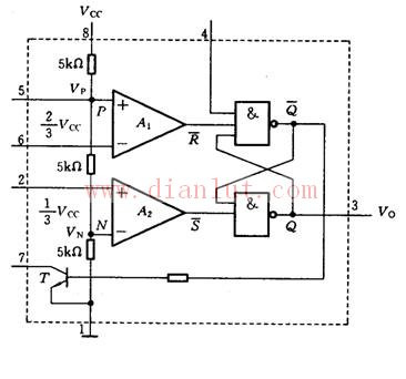
(1) Voltage divider: The voltage divider is composed of three 5kΩ resistors in series. The upper end is connected to the power supply VCC (8 terminals) and the lower end is grounded (1 terminal) to provide the reference level for the two comparators A1 and A2. The "+" terminal of comparator A1 is connected to the reference level of 2VCC/3 (5 terminals), and the "-" terminal of comparator A2 is connected to VCC/3. If the control voltage is applied to the control terminal (5 terminals). The reference levels of the two comparators can be changed. When the control voltage is not applied, the 5-terminal AC ground can be grounded with a 0.01μF capacitor to bypass high-frequency interference.
(2) Comparators A1, A7 are two comparators. Its "+" end is the in-phase input terminal, and the "-" end is the inverting input end. Because the sensitivity of the comparator is very high, when the level of the non-inverting input is slightly larger than the inverting terminal, its output is high; otherwise, when the level of the non-inverting input is slightly smaller than the level of the inverting input, its output is Is low. Therefore, when the trigger level of the high-level trigger terminal (6-terminal) is greater than 2VCC/3, the output of the comparator A1 is low; otherwise, the output is high. When the trigger level of the low-level trigger terminal (2 terminal) is slightly smaller than VCC/3, the output of comparator A2 is low; otherwise, the output is high.
(3) Basic RS flip-flop: The outputs of comparators A1 and A2 are the input terminals RD and SD of the basic RS flip-flop. Therefore, the state of the basic RS flip-flop (the state of the 3-terminal) is controlled by the input levels of the 6-terminal and the 2-terminal. The 4 terminals in the figure are low-level reset terminals. When a low level is applied to the 4 terminals, the reset can be forced to make Q=0. Normally, the 4 terminal is connected to the positive terminal of the power supply VCC.
(4) In the discharge switch diagram, the transistor VT constitutes a discharge switch. When used, the collector is connected to the positive power supply, and the base is connected to the Q terminal of the basic RS flip-flop. When Q=0, VT is turned off; when Q=1, VT is fully turned on. It can be seen that the transistor VT acts as a discharge switch, and its on-off state is determined by the state of the flip-flop.
Big Size Switch And Socket,Big Size Switch,Big Size Socket,Big Size Switch Socket For Sale
ZHEJIANG HUAYAN ELECTRIC CO.,LTD , https://www.huayanelectric.com