At present, there are usually two methods for loading: one is to use a dedicated cable to load data through the JTAG port, and the other is to externally mount a PROM chip that is compatible with the FPGA manufacturer. The former needs to run dedicated loading software on the PC and download it directly into the FPGA chip. Therefore, the power-down data will still be lost. It is only applicable to the FPGA debugging phase and cannot be applied to the data loading in the industrial field. Although the latter can solve the problem of data loss, the cost of this special chip is relatively high, and the lead time is also long (generally more than 2 months), which makes the development time of FPGA products greatly constrained. According to the FPGA chip loading timing analysis, this paper proposes to replace the dedicated PROM by the common Flash ROM chip on the market, and carry on the FPGA loading through the external high-speed bus of the DSP; it not only saves the system cost, but also can quickly load the FPGA. Purpose; especially suitable for the stage of the program to be solidified in the later stage of FPGA debugging. Let's take two Xilinx Virtex-4 series XC4VLX60 chips as an example to introduce the hardware and software design of TI's TMS320C61416 DSP to control FPGA chip data loading .
1 Xilinx FPGA Configuration Principle
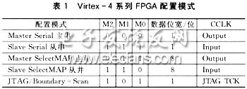
Virtex-4 series FPGA chip external configuration pin MODE PIN (M0, M1, M2), there are five configuration modes, as listed in Table 1.
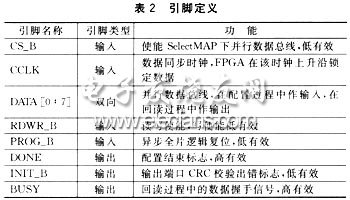
In the Slave SelectMAP mode, the FPGA shares the 15 configuration pins listed in Table 2.
1.1 Configuration Process
The FPGA loading timing is shown in Figure 1. Each configuration signal must meet its timing relationship, otherwise the configuration work cannot be completed normally.

In Figure 1, the Slave SelelctMAP load mainly includes the following three steps:
1 start and initialize. After the FPGA is powered up normally, the asynchronous reset of the FPGA is performed by the low pulse of the PROG_B pin, so that the internal logic of the FPGA is cleared. Secondly, PROG_B is pulled high to stop the external reset. The INIT_B pin will automatically generate a low-to-high transition during the TPOR period, indicating that the FPGA internal initialization is complete and data can be downloaded. At the same time, the FPGA samples its rising edge on INIT_B. The mode pin MODE PIN determines its mode configuration.
2-bit stream loading. After the INIT_B signal goes high, no additional latency is required and the Virtex device can begin data configuration immediately. Bitstream data is placed bytewise on the rising edge of the external CCLK signal. The process includes four parts: synchronous initialization word, device ID number check, load configuration data frame, and CRC check.
3STARTUP starts. After successfully verifying the CRC code bits, the bitstream command causes the FPGA to enter the STARTUP state. It is implemented by an 8-phase state machine. The middle includes waiting for DCM phase lock, DCI matching and other states. Finally, the FPGA releases the external DONE pin, and the external output is high impedance state, which is pulled up externally to indicate that the FPGA is successfully loaded.
1.2 File generation
There are three main types of ISE generated data files: BIT files, which are characterized by binary format logic design, including file header and configuration data, mainly used for JTAG download cable mode; MCS files, download files generated for external PROM, ASCII code Different from the former, it contains the data address and check value in the PROM; the BIN file format, represented by binary, consists entirely of configuration data, and does not require other extraction and hex conversion, just the Byte before configuration. Swapped is implemented in CPLD. This design uses the BIN file format.
2 hardware implementation
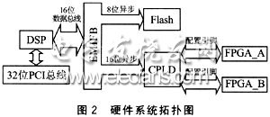
The system uses two Xilinx Virtex-4 series of 6 million gate FPGA XC4VLX60. The main MCU is TI's high-performance fixed-point processor TMS320C6416, which has two external EMIF bus interfaces, 64-bit wide EMIFA and 16-bit wide EMIFB. There are 8 8MB Flash and 16-bit CPLD on EMIFB: Flash is used to save BIN files of 2 FPGAs, which were previously programmed by the emulator; CPLD is used for 2 FPGA address decoding and logic interface between DSP and FPGA configuration. The entire data flow is after the DSP is powered on, the bootloader boots the user program. This program is responsible for moving the BIN file in the Flash space by the EMIFB bus, and configuring and loading two FPGAs through the CPLD. The hardware system topology is shown in Figure 2.
3 software design
The software consists of three parts: the bootloader code, the FPGA user program, and the CPLD Verilog code in the interface section.
3.1 DSP Bootloader
In this system, the target board is in the late stage of FPGA debugging, and its loader needs to be solidified. After the whole board is powered, it is required to load the FPGA from the emulator itself, so the EMIF BooT method of DSP is used here. After the power-on reset of the DSP, the first 1 KB of the ROM space of the BCE1 is moved to the chip by EDMA by default in the default ROM timing, and the operation starts at its 0x0 address.
Generally, the program code written by C is much longer than 1 KB. If you just move the first 1 KB of Flash from the DSP, you will lose data and the program will not work properly. Here a two-shifted bootloader program written in assembly language is used to guide larger user programs. The assembly language is used because of its high code efficiency and short code length (only 256 bytes in this system). The two moves are because the Bootloader after the first DSP self-movement will occupy the first 1 KB of the 0x0 address on the chip, and conflict with the next user program 0x0 address copy (the interrupt vector table must be placed at the 0x0 address, otherwise the interrupt will be lost. The absolute address of the jump), and the running bootloader cannot overwrite itself. So the part of the code that copies the user program is placed on the bottom of the chip to run, freeing up the 0x0 address of the user space. After the final copy is complete, the bootloader jumps to the user program entry address c_int00 to run.
When you get into trouble, for example, dark, emergency or outdoor activities. You must be need a Cob Aluminum Flashlight. Our products have 1-5 modes, the modes of every COB Aluminum Flashlight can customized. Usually, people prefer 3 modes;
Our products equipped with new COB LED technology, some products have a zoomable feature, you can ajust its focal distance according to your demand;
The anodized aluminum body and recessed LED housing ensures that the COB Aluminum Flashlight can handle any situation.
All of the flashlight have simple on/off push button operation;
COB Aluminum Flashlight for emergency events, camping, outdoor activities and indoor, due to the products have high power, they can irradiate long distance;
Our products are saled with factory price, and the quality can guarantee, lastly we provide warranty for 1 year.
COB Aluminum Flashlight
18650 Tactical Flashlight,Cob Aluminum Flashlight ,Cob Aluminum Torch,T6 Tactical Flashlight
Ningbo Henglang Import & Export Co.,Ltd , https://www.odistarflashlight.com