Pick   Important : This article introduces the performance characteristics and design considerations of the ADS5500 , and gives a brief description of its application in video signal processing.
Overview
In recent years, with the rapid development of digital signal processing technology and the continuous emergence of new theories and new algorithms, coupled with the overall improvement of the performance of digital signal processing devices, the actual system has become increasingly demanding on analog-to-digital converters. Therefore, in practical applications, it is generally required that the analog-to-digital converter must have a high sampling rate and accuracy, a large dynamic range, an extremely wide frequency response range, and a flexible digital interface.
ADS5500 is a high-performance analog-to-digital converter developed by TI with 14 -bit resolution and 125MSPS sampling rate. The chip is packaged in 64- pin TQFP PowerPAD . In order to achieve a higher degree of system integration, it also includes a wide bandwidth linear sample / hold and a complete conversion solution of the internal reference voltage source. At 100MHz , the signal-to-noise ratio (SNR) of the ADS5500 is 70dB , the distortion-free dynamic range (SFDR) is 82dB , the differential input voltage is 2.2Vpp , the operating voltage is 3.3V ( unipolar ) , and the power consumption is only 750mW . The internal reference voltage source simplifies the system design, and the parallel CMOS compatible data output interface ensures a seamless connection with common logic circuits and facilitates connection with digital signal processors. The internal structure diagram is shown in Figure 1 .

Picture 1 Â ADS5500 internal structure block diagram

Picture 2 Â ADS5500 working signal timing
Picture 3 Â Analog input section
Design considerations
ADS5500 is a low power, 14-bit sampling rate 125MSPS pipelined analog to digital converter, only a single polarity power supply of 3.3V can work properly. The data conversion process starts at the rising edge of the clock signal waveform. Once the analog signal is captured by the sample / hold part of the converter, the sampling process of the input signal is sequentially divided into a series of pipeline operations to make the rising and falling edges of the clock signal Data conversion can be carried out along the way. It takes 16 clock cycles of delay from inputting analog signals to outputting 14 -bit data . Figure 2 shows the corresponding timing of ADS5500 input, output signal and clock waveform.
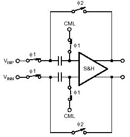
Input configuration
The analog input part of the ADS5500 is mainly composed of a differential tracking / holding amplifier and switched capacitors ( Figure 3) .
Differential input technology ensures high performance under high sampling rate conditions, but also brings a very high available input bandwidth, which is particularly important for some IF sampling or undersampling applications.
For the input configuration of low-frequency input signals, differential input / output amplifiers ( such as OPA695) can be used to simplify the front-end drive circuit. The advantage of this configuration is that it has greater flexibility, the amplifier can be used to complete the analog input signal polarity conversion ( unipolar to differential ) , signal amplification and ADC front-end pre-filtering and other work.
Reference source circuit
The internal reference voltage source of the ADS5500 simplifies the circuit layout of the circuit board. For this, no additional circuits are needed on the board. But from the perspective of optimizing performance considerations, can be connected to a respective capacitor in 1mF REFP and REFM pins and grounded. Further, in order to better set the operating current of the chip, is also connected to a 47 Ω resistor in the IREF pin, and is connected to pin AGND (FIG. 4).
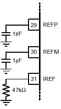
Picture 4 Â REFP , REFM and IREF pins optimize system performance
Picture 5 Â Clock input signal pin connection circuit

Figure 6 ADS5500 to build a real-time image processing system
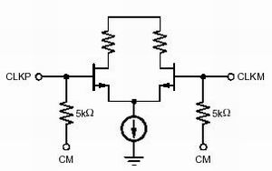
Clock input signal
The clock input signal of the chip can be unipolar or differential. In normal mode, the voltage amplitude of the clock input signal is set to 1.5V , and the CLKP pin and CLKM pin are connected to the CM pin through 5k Ω resistors ( Figure 5 ) .
From a practical point of view, selecting a low-jitter clock source and performing corresponding band-pass filtering on it can greatly improve the performance of the high-frequency sampling system. The ADC core inside the chip can perform data conversion on the rising and falling edges of the clock signal waveform, further improving the working efficiency of the chip. When there is no clock source or the clock frequency is lower than 10MSPS , the chip will automatically switch to sleep mode.
Output options
The chip generates 14 -bit data output signal (D13-D0) , 1 data ready signal (CLKOUT pin ) and 1 data overflow indicator bit (OVR pin, when the output data amplitude exceeds the maximum value, this bit is set Is 1) .
The data format of the output signal and the polarity of the clock output signal can be set by changing the DFS pin level. The data format of the output signal has two forms: direct binary code and two's complement, and the clock polarity is that the output data is valid at the rising or falling edge of the clock waveform. There are four selection ranges for the DFS pin level, so there are four correspondences. Table 1 shows the correspondence between these four modes.
Application examples
Figure 6 is a real-time image processing system. The CCD sensor sends the original image ( analog signal ) to the ADS5500 high-frequency sampling to obtain a high-precision digital image signal, which is then sent to the image processing unit through the high-speed synchronous FIFO , which is processed by the digital signal processor Complete the image processing and compression, and display the processed data on the LCD or CRT display.
Conclusion
The ADS5500 interface is simple, easy to use, flexible, 14 -bit sampling accuracy, and at the same time has a high conversion speed. In most applications that require high-speed data acquisition and high-precision measurement, the chip has strong practicality.
Zoom Camera , Thermal Camera ,Drone searching Light, Drone Mega Phone,Drone Survey Gimbals
Zoom Camera, Thermal Camera,Drone searching Light, Drone Mega Phone,Drone Survey Gimbals
shenzhen GC Electronics Co.,Ltd. , https://www.jmrdrone.com