Abstract: According to the IRDA infrared serial physical layer specification IRDA-1.4, a very high-speed VFIR infrared controller based on PCI bus is designed, and the hardware and software design methods and implementation process of the controller are analyzed in detail. In the design, the PCI bus main control interface chip S5933 is used to realize the conversion of the complex PCI bus interface to a relatively simple user interface function; the FPGA is used to realize the transmission control and sequential logic of the infrared controller.
PCI (Peripheral Component Interconnect) local bus [1] is a high-performance, 32-bit or 64-bit address data multiplexing synchronous bus. Its purpose is to provide an internal connection mechanism between highly integrated peripheral control devices, expansion cards, and processor / memory systems. It specifies the protocol, machinery, and equipment configuration space of the interconnection mechanism. The PCI local bus is favored by the industry for its features of minimal delay time, support for linear burst data transmission, compatible performance, and fully automatic configuration of the system. Version 2.1 of the PCI bus specification also defines a method of expanding from a 32-bit data bus to a 64-bit bus, to expand the bus width, and to achieve forward and backward compatibility with 32-bit and 64-bit PCI local bus peripherals.
At present, infrared communication between computers is based on the infrared wireless serial SIR communication based on the IRDA-1.1 standard. Reference [2] gives the design and implementation of an infrared wireless serial communication card based on the ISA bus. The data rate of the communication card It is 9.6kbps ~ 115.2kbps, and the working distance is 0 ~ 3m. However, because the upper limit of the maximum data rate of the RS-232 port is 115.2 kbps, which cannot meet the IRDA-1.4 specification of the very high-speed infrared VFIR 16Mbps rate requirements, the PCI synchronous bus is used to design the very high-speed infrared controller. Although the transmission rate of the ISA bus can meet the design requirements of the very high-speed infrared controller, many microcomputer systems have gradually eliminated the ISA / EISA standard bus. The reason is that the high-speed microprocessor and the low-speed ISA bus are not synchronized, which causes the extended peripherals to send and receive data only through a slow and narrow bottleneck, which seriously affects the high performance of the CPU. 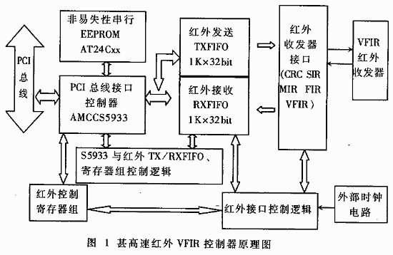
1 HHH (1,13) codec
In May 2001, the Infrared Wireless Data Association IRDA released the infrared serial physical layer specification IRDA-1.4 [4]; the main difference between it and the physical layer specification released in the previous period is the addition of a very high-speed infrared VFIR 16Mbps data rate encoding and decoding technology and Frame structure, while other specifications such as viewing angle range, minimum (large) optical power of transmitter and receiver sensitivity are based on the same. Infrared serial physical layer specification IRDA-1.4 stipulates that data rate less than 4Mbps adopts RZI (return to zero inversion) modulation, and the maximum pulse width is 3/16 or 1/4 of the bit period; data rate 4Mbps adopts 4PPM (pulse position modulation); The data rate of 16Mbps uses HHH (1, 13) code.
The VFIR codec technology proposed by IRDA-HHH (1,13) code is a RLL (run-length-limited) code with a code rate of 2/3, (d, k) = (1,13); it is a power Efficient coding with relatively compromised consumption and frequency band utilization, where parameters d and k represent the number of minimum and maximum '0' between two '1's respectively, parameter d determines whether there is inter-symbol interference ISI in the received signal, parameter k determines whether the receiver can recover the clock from the received sequence. The bandwidth efficiency of the HHH (1,13) code allows data communication to select LEDs with a low cost and a rise / fall time of 19ns. The power efficiency avoids the thermal problem of LED, it can guarantee to keep the link within 1m distance. A 16 Mbps link at a distance of 1 m can reach the drive current and power consumption of a link of 4 Mbps in the past. The significant difference between the HHH (1,13) code and the 4PPM code (for 4Mbps) is that the HHH (1,13) code never allows an infrared pulse to follow the previous infrared pulse, and a chip time difference should be maintained between the pulses. Due to the slow radiation of a small number of carriers in the working area of ​​the phototube, the LED or photodiode exhibits a tailing effect, and the HHH (1,13) code is compatible with the tailing effect, thereby allowing pulse expansion within the chip time period .
Although the design process of the HHH (1,13) code is more complicated, the IRDA-1.4 standard has already given the compiled code logic equations and circuits in detail, so it is easier to implement. The author uses Altera MAX + plus II for logic function simulation, and uses GW48 EDA experimental system for hardware authenticity to verify the correctness of the HHH (1,13) code compilation circuit design. 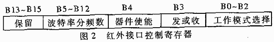
2 Very high-speed infrared VFIR controller hardware design
Because the PCI bus stipulates strict electrical characteristics, it is very difficult to develop the application of the PCI bus. Therefore, the PCI interface controller S5933 introduced by the AMCC (Applied Micro CorporaTIon) company is used to implement the PCI bus interface specification of the infrared controller [5]. The functional block diagram of the very high-speed infrared VFIR controller is shown in Figure 1. Use Altera's FLEX10K series field programmable gate array device to realize the transmission control and logic timing of S5933 and infrared TX / RXFIFO, registers, infrared interface control logic and infrared transceiver interface function modules (CRC check, codec and serial / parallel Conversion). The working principle of the very high-speed infrared VFIR controller is as follows: First, the PCI configuration space is downloaded by the AMCC S5933 external non-volatile serial EEPROM AT24C02, and then the host writes control commands to the infrared interface control register through the pass-thru (PassThru) register data access method [3] . The infrared interface control logic sends out control signals according to the control commands, so that the entire infrared controller is in a ready state. When the upper layer protocol sends a data transmission event, the infrared interface control logic sends a message to inform the host to start the S5933 bus master read operation, and write the upper layer data to the external infrared TXFIFO data buffer; at the same time, the infrared interface control logic sends the TXFIFO data according to the TXFIFO status Send to infrared transceiver interface, latch, parallel / serial conversion, CRC checksum coding, and finally send data through VFIR transceiver. Similarly, the data received by the VFIR transceiver is decoded, CRC checked, serial / parallel conversion and latched, and written into the RXFIFO data buffer. The infrared interface control logic triggers the upper layer protocol to send a data reception event to receive data. The host initiates the S5933 bus master write operation to submit data to the upper layer protocol. After the data transmission is completed, the upper layer protocol sends a message back to notify the data reception completion. The following focuses on the analysis of S5933 and infrared TX / RXFIFO, infrared register bank access control logic, infrared interface control logic and infrared transceiver interface functions.
2.1 Infrared TX / RXFIFO and infrared control register group control logic
AMCC S5933 supports 3 physical bus interfaces: PCI bus interface, expansion bus interface and non-volatile EEPROM bus interface. Non-volatile EEPROM is used to map the configuration space of PCI and the initialization of the device BIOS; the expansion bus can be interconnected with peripheral devices. S5933 mailbox register, FIFO register, pass-through register (Pass-Thru) data transmission method can be used to transfer data between the host and peripherals.
The infrared register set includes an infrared interface control register and a status register. In this paper, very high-speed infrared control uses the S5933 pass-through register single-cycle data transfer to write the control word to the infrared interface control register. The pass-thru logic control circuit separates the address and data. The pass-through address register (APTA) is latched and decoded by 374 , Select the infrared interface control register, and write the low word of the pass-through data register (PTDA) to the infrared controller; the data width of the interface control register is 16 bits, including the infrared controller's initial energy and working mode (UART, SIR, MIR, FIR, VFIR) settings, the choice of receiving or sending data and the frequency division number that meets the multi-baud rate in SIR mode. Infrared interface control register structure definition is shown in Figure 2.
Similarly, the pass-through register mode is used to obtain the status of the infrared interface status register. Infrared interface status register structure definition is shown in Figure 3. 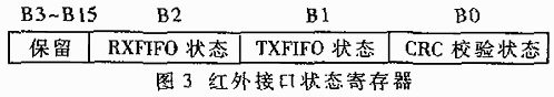
In order to meet the high-speed data transmission, the synchronous burst (Burst) operation (DMA transfer) under the main control mode of the S5933 FIFO register bus is used to complete the data transmission between the host and the infrared TX / RXFIFO. The PCI interface first initializes S5933 as a bus master device, and then the PCI interface writes the address of the PCI storage space to be accessed to the master read / write address register (MRAR / MWAR), and writes to the master read / write counter (MRTC / MWTC) Write the number of bytes to be transferred. S5933 provides 4 dedicated pins RDFIFO #, WRFIFO #, RDEMPY # and WREULL # to control the data transmission interface logic of internal FIFO and external FIFO. The data width of the receive / send FIFO is 32 bits, which are respectively realized by the IDT72220 FFO data bit expansion of 4 8-bit data buses. The FIFO provides both data buffering for the PCI interface and access data for the infrared transceiver interface. The data access control logic of S5933 and infrared TX / RXFIFO and infrared register group is shown in Figure 4.
2.2 Infrared interface control logic
According to the control words of the infrared interface control register, the infrared interface control logic implements data transmission and logic timing between the external RX / TXFIFO and the infrared transceiver interface. Its working principle is as follows: According to the control word, first start the infrared transceiver interface CRC check, codec and programmable clock (RX / TXFIFO read / write clock RCLK, WCLK and codec clock fclock), then according to the control word The TX / RX bit determines whether to receive or transmit data. When sending data, the TXFIFO buffer is not empty, the TXEF EF signal triggers the infrared interface control logic to send the TXFIFO read operation signal ENR #, read the TXFIFO data (data width 32 bits) and pass it to the infrared transceiver interface for CRC check , Encoding and parallel / serial conversion. Similarly, when the very high-speed infrared controller receives data, the data received by the infrared transceiver undergoes decoding, serial / parallel conversion (data width 32 bits), and then triggers the infrared interface control logic to send the write operation signal ENW # of the infrared receive FIFO Write the received data to the infrared receive FIFO. When the RXFIFO is full, the control logic is triggered to send out the S5933 FIFO write signal WRFIFO #, and the upper layer protocol starts the PCI interface to initialize S5933 to realize the data transfer from the infrared receiving FIFO to the host memory for the synchronous main control write operation. In addition, the infrared interface logic also realizes the configuration of the status register of the infrared interface to facilitate the upper layer protocol to understand the working status of the infrared controller.
2.3 Infrared transceiver interface
The design and implementation of the infrared transceiver interface is the key to the success of the infrared controller. The interface needs to implement various codecs (SIR, MIR, FIR, VFIR) codec and hardware CRC check, the design is more complicated. Before the encoder and after the decoder, the data should be checked by hardware CRC to realize error control. SIR mode adopts RZI (Return to Zero Inversion) coding, the signal is high level and the modulation is low level; the signal is low level and the modulation is high level pulse, and the maximum pulse width is 3/16 of the bit period. The MIR mode also uses RZI (Return to Zero Inversion) encoding, but the maximum pulse width is 1/4 of the bit period. The FIR mode uses 4PPM (Pulse Position Modulation) modulation. Its principle is that every two bits of the encoded binary data stream are combined into a data symbol group (DBP) with an occupation time of Dt = 500ns, and then the data symbol group ( DBP) is divided into four 125ns time slots (chip), according to the state of the symbol group, single pulses are placed in different time slots. Because PPM communication relies on the position of the signal light pulse in time to transmit information, so when demodulating, ensure that the time slot synchronization and frame synchronization of the sender and receiver, and then demodulate the transmission data according to the position of the pulse in the 500ns period. Considering that the sudden change of the communication distance of the infrared transceiver causes the pulse width to expand, the inter-symbol interference occurs, and the decoding error occurs. Therefore, according to the new algorithm proposed by Hiroshi Uno [7], the 4PPM decoding process is simplified, and the algorithm is verified by experiment However, the decoding algorithm has a simpler structure, lower power consumption, and is easier to implement.
The VFIR mode uses HHH (1, 13) codec technology. The principle of the encoder: In order to achieve the correct encoding, it is required that the input data symbol group d = (d1) that reaches the input end of the encoder at nT (T represents a chip time) before calculating the internal code word C = (c1, c2, c3) , d2) After a delay of 3 encoding cycles (each encoding cycle is 3T), a logical calculation is performed to obtain the next state vector value N = (s1, s2, s3), that is, N related to the input data appears in ( n + 9T) time; after another encoding cycle, namely (n + 12T) time, state N is assigned to the internal state vector S = (s1, s2, s3), and the data group d = (d1, d2) The relevant internal code word vector C = (c1, c2, c3), and after another encoding cycle, the internal code word C is assigned to the output code word vector Y = (y1, y2, y3). It can be seen that the data rate of 16Mbps becomes 24Mchip / s encoding rate through the encoder, and the entire encoding process is delayed by 5 encoding cycles, that is, 15 chips. Note that the initial state S of the encoder should be set to (1, 0, 0). Decoder principle: The input data R = (r1, r2, r3) obtains the vector Y4 = (y10, y11, y12) through the delay of the latch, and Y3, Y2, and Y1 are obtained by delaying Y4 differently. Here, the vector Yi is the 4-I time delay of Y4 (the delay is realized by the latch); Zd is obtained by performing the NOR operation on Y4, and then Zd is subjected to different delays to obtain Zc and Zb. Here Zc, Zb, Zd are variables, and then Y4, Y3, Y2, Y1, Zb, Zc, Zd are logically operated and delayed to obtain vectors X1 = (x1, x2), X2 = (x3, x4), X3 = (x5, x6); Finally, the x1, x2 pass the latch to get the decoder output vector value U = (u1, u2). The entire decoding process is delayed by 4 cycles or 12 chips. It can be seen that the HHH (1, 13) coding and decoding circuit is relatively simple, which can be realized based on the gate-level description using FPGA, but it must be noted that the latch clock fclock = 1 / 3fchip. VFIR mode adds a linear feedback shift register (LFSR) to achieve scrambling and descrambling functions to improve system performance and reduce bit errors.
Figure 4 S5933 and infrared receive / transmit FIFO, infrared register group data access control logic diagram
3 Very high speed infrared VFIR controller software design
The controller software is mainly divided into three parts: system initialization part, receiving part and sending part. System initialization first calls the BIOS 1Ah interrupt function to obtain the device PCI bus number, function number, memory, I / O space base address and space size, and interrupt number, and then writes the control command to initialize the infrared controller through Pass-Thrn mode, select The controller receives or sends data, sets the controller working mode and baud rate frequency division number, and allows the controller to work. The infrared controller has the ability to send and receive bidirectional data transmission. When programming, set the S5933FIFO to be initialized by the PCI interface as a synchronous master control mode to support burst transfer (DMA); then determine whether the PCI bus master read or master write operation according to the controller receive / send bit. The program uses interrupt control. The main program calls set_up_pci_busmaster () to initialize the master control operation. This function not only loads the actual address of the access memory and the number of transmitted bytes, but also allows reading / writing the number of transmitted bytes to zero interrupt. After the infrared controller is initialized, the system waits for an interrupt. The interrupt service handler reads the S5933 interrupt status / control register INTCSR to determine the source of the interrupt and clears the interrupt flag; reads the CRC check status bit to determine whether the received data is correct. When sending data, the interrupt service handler also checks whether the infrared transmit FIFO status bit is 1 (1 indicates that the FIFO is empty). If it is not set to 1, the send non-empty flag tx_not_empty = 1. The main program continues to wait until the TXFIFO data is For the same reason, to receive data, it is also necessary to detect whether the red receive FIFO status bit of the infrared interface status register is 1 (a test bit of 1 indicates that the FIFO is empty). This ensures that the data in the receive and transmit FIFO is completely taken away. The written application is debugged with Turbo C2.0.
The PCI bus has become the mainstream bus of today's computers. Therefore, a very high-speed infrared VFIR controller for the basic PCI bus is designed according to the infrared serial physical layer specification IRDA-1.4. Use the AMCC company PCI bus special controller plus some interface control circuits to realize the VFIR controller hardware design, shorten the development cycle, improve efficiency, and save costs. Currently using VtoolsD to develop virtual drivers to solve how the system allocates infrared controller configuration resources, how to access hardware devices, how to handle hardware interrupts and bus master DMA operations, and communication between VXD and applications. In addition, foreign companies have launched special chips for VFIR infrared controllers, such as MK7100 from MKNET.
The USB HUBS is also known as a port replicator which is an external device designed for laptop computers. By copying or even extending the port of the notebook computer, the notebook computer can be easily connected with multiple accessories or external devices (such as power adapter, network cable, mouse, external keyboard, printer and external monitor) in one stop.
The USB C Hubs has both the functionality of a port replicator and is used to extend to a considerable degree of desktop functionality. Especially suitable for professionals, such as the need for more interface equipment. Using the laptop docking station for company, home or business presentations can also increase the ease of use and excellent scalability of the notebook. For example, consider using the UltraBay interface on the docking station to obtain an optical drive, burner, battery, numeric keypad, hard disk and other expansion functions.
The biggest use of the mini Type C Usb Hub is port expansion. As it is known to all, laptop computers are much less than desktop computers due to their own size limitations, both in terms of the number of ports and types, and sometimes it is difficult to meet the needs of users. The mini dock, on the other hand, offers multiple port extensions, like a laptop that suddenly has three heads and six arms. Some ports are most laptops do not have their own, such as serial port, PS/2, DVI, IBM dedicated floppy drive port. Some are more numerous than the body of a laptop, such as USB ports. These numerous ports allow the laptop to connect to more peripherals at the same time, improving the performance of the entire laptop and helping to increase productivity.

Usb Hubs,Multi Usb Adapter,Usb C Desktop Hub,Usb 3.0 Multi Port Hub
Henan Yijiao Trading Co., Ltd , https://www.yjusbcable.com