Ron Wilson, Altera Corporation
The pursuit of memory bandwidth has become the most prominent theme of system design. SoC designers whether using ASIC or FPGA technology, the core of their thinking is the need to plan, design and implement memory. System designers must clearly understand the memory data flow patterns and the ports established by the chip designer. Even memory vendors face DDR exits, and they must understand system behavior in order to find new ways to continue development.
At the hot chip conference held at Stanford University, the search for bandwidth became the topic of the paper's discussion. The designers introduced many methods to solve the challenges. From these articles, and from the experience of designers working in the field, it can be seen how memory system architecture will evolve in the future.
Memory barrier
The basic problem is clear: Modern SoC clocks are as high as gigahertz and have multiple cores, which will generate more memory requests per second than single-channel DDR DRAMs. If so, there will be obvious solutions to this problem. However, there are important fine structures behind this, which make this problem very complicated and lead to various solutions.
The focus of SoC developers has shifted from high-speed clocks to multiple cores, which has fundamentally changed memory issues. No longer is it a requirement for a CPU to have higher megabytes per second (MBps), and now we are facing many different processors - often many different types of processors, all requiring simultaneous access. Moreover, the main mode of memory access has changed. Scientific and commercial data processing tasks often involve large amounts of local access or, worse still, a relatively slow transfer of large amounts of data using a relatively compact algorithm. Configuring a moderately-sized local SRAM or cache, a CPU for such tasks does not have a high requirement for main memory.
DRAM chip designers take advantage of this ease of use to achieve higher density and energy efficiency. Correspondingly, when applying large blocks of data in a predictable order, DRAM achieves the best bit rate - it allows block interleaving. If the SoC does not use this common mode, the effective bandwidth of the memory system can be reduced by an order of magnitude.
New access mode
The bad news is that the development of SoC makes it difficult for DRAM designers to make assumptions. New trends in multithreading and software design have changed the way each core accesses memory. Multi-core processing and increasingly important hardware acceleration mean that many hardware are competing for main memory. These trends make simple local access complicated and DRAM bandwidth is related to this.
Multi-threading means that when a memory application misses its cache, the CPU does not wait: it starts executing different threads, and its instruction and data areas are in a completely different physical memory area than the previous threads. Careful multi-path cache design helps solve this problem, but in the end, continuous DRAM applications are still very likely to access irrelevant storage areas, even though each thread carefully optimizes its memory organization. Similarly, multiple cores competing for the same DRAM channel also disturb the DRAM access sequence.
Changes in the software can also have an impact. Table lookup and link table processing generates randomized, decentralized memory accesses to big data structures. Packet processing and big data algorithms move these tasks from control code to high-volume data processing. System designers have to specifically consider how to handle them efficiently. Virtualization puts many virtual machines in the same physical core, making memory data flow more complex.
Traditional solutions
These problems are not new issues - they just become complicated. Therefore, chip and system designers have many mature methods to meet the increasing demand for baseband bandwidth and improve DRAM access efficiency. These methods include software optimization, caching, and the deployment of multiple channels of DRAM.
Most embedded system designers are accustomed to think of software optimization first. In a single-threaded system, software uses memory channels to a large extent and consumes a lot of energy. However, in multi-threaded, multi-core systems, software developers have little effect on the actual sequence of events on the DRAM controller. Some experience shows that it is difficult for them to change the actual runtime data flow pattern. DRAM controllers can use reordering and fairness algorithms, which programmers are not aware of.
The cache is more efficient - if the cache is large enough, it can significantly reduce DRAM data flow. For example, in an embedded multi-core implementation, a relatively small L1 instruction cache works with a moderately-sized L2 to fully accommodate all thread hotspot codes, effectively reducing the amount of instruction fetching data flow to the main memory. Similarly, in signal processing applications, relatively little data is fit into L2 or local SRAM, which can remove the filter kernel load. To make a big impact, caching doesn't have to actually reduce the total number of DRAM requests - it only needs to protect the main source of the application from being interrupted by other tasks, so the programmer can optimize the main tasks.
When chip designers cannot determine the various tasks that will be run in the SoC, they tend to provide as much cache as possible, as costly as possible: L1 cache for all CPU cores and accelerators, large-scale sharing of L2, and more The larger die L3. At the hotspot chip conference, there are many cached instances from tablet-level application processors to a large number of server SoCs.
At the low end, AMD's Kabini SoC (Figure 1) is an interesting study. AMD senior researcher Dan Bouvier introduced the chip, which includes four Jaguar CPU cores that share 2 megabytes (MB) of L2 cache, and each Jaguars has 32 kilobytes (KB) of instruction and data caches— - Not a non-traditional agreement. Even more amazing is the chip's graphics processor, in addition to the usual color cache and Z buffer for the rendering engine, as well as its own L1 instruction cache and 128 KB L2.

Figure 1. AMD's Kabini SoC target application is a tablet, but still uses a large-scale cache, significantly increasing the memory bandwidth.
At the high end is IBM's POWER8 microprocessor (Figure 2), and IBM chief network architect Jeff Stuecheli introduced the chip. The 650 mm2, 22 nm chip includes 12 POWER architecture CPU cores, each with 32 KB instructions and a 64 KB data cache. Each core also has its own 512 KB SRAM L2 cache, and 12 L2 shares a large 96 MB embedded DRAM L3. Stuecheli said that the three-level continuous cache supports a total memory bandwidth of 230 gigabytes per second (GBps). Interestingly, the chip also contains a small-capacity session memory.
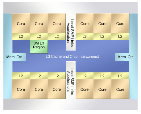
Figure 2. IBM's POWER8 architecture implements L3 cache on the SoC die.
Between the two SoCs is a multi-die module for Microsoft's XBOX One (Figure 3), which was introduced by Microsoft's John Snell at the conference. The module contains a SoC die, providing a wealth of memory resources. The SoC has eight AMD Jaguar cores divided into two groups of four. Each core has 32 KB of L1 instruction and data cache. One 2 MB L2 is shared by every 4 CPU cores. In addition, there are four 8 MB shared SRAMs on the die that provide at least 109 GBps of bandwidth for the CPU.
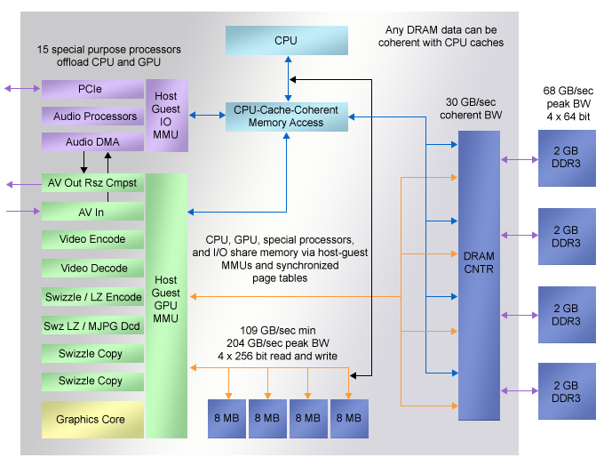
Figure 3. Microsoft's XBOX One combines large-capacity caches, local SRAM, and in-module DRAM to achieve greater bandwidth at a lower cost.
Use DRAM
The XBOX One SoC also reveals more information. No matter how big die cache you have, it cannot replace the huge DRAM bandwidth. The SoC die includes a quad-channel DDR3 DRAM controller that provides 68 GBps of peak bandwidth for 8 GB of DRAM in the module.
The concept of DRAM multi-channel is not limited to gaming systems. A few years ago, the packet processing SoC began to provide multiple fully independent DRAM controllers. However, this strategy has brought challenges. Memory optimization will be more complex, and system designers must decide which data structure maps which channel or controller. Of course, it is also possible to require your own DRAM controller to perform some of the most demanding tasks. In some embedded applications, these controllers are invaluable. The DRAM multi-channel will quickly run out of pins, exhausting the I/O power budget.
Even in FPGA design, the pin count is a problem. Designers should be able to re-organize the logic very flexibly and choose a larger package. Altera's Advanced System Development Kit (Figure 4) board is primarily used for prototyping and implementing broadband designs. Applications include HD video processing, Layer 7 packet inspection, or scientific computing. This is a very useful package.
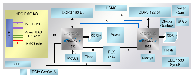
Figure 4. Altera's advanced system development kits greatly satisfy the memory requirements of two large-scale FPGAs.
Mark Hoopes, an Altera Broadcast Application Specialist, explained that boards should provide a large memory bandwidth and do not require detailed knowledge of certain designs that users implement in two large-scale FPGAs. Therefore, when designing the board, Hoopes examined the existing memory usage pattern of Altera's video intellectual property (IP) and investigated the needs of the external design team.
The result is sobering. Hoopes said: "When you look at each feature, it looks like it needs storage. However, when you combine the features, the demand is very large. In one example, the application developer requires that every FPGA be provided The 256-bit wide DDR3 interface and the quad QDR II SRAM are not even possible in a 1932-pin package, so designers eventually used four SRAM blocks and a 192-bit DDR3 interface.
Hoopes pointed out that multiple memory controllers are very important for SoCs. He said that IP developers are usually skilled at optimizing memory at the subsystem level and can even provide their own optimized DRAM controllers. It is also possible to have a DRAM channel dedicated to the subsystem, allowing other IP modules to run subsystem designer optimizations.
future development
There is another interesting module on the development board: One MoSys bandwidth engine is connected to each FPGA. The chip contains 72 MB of DRAM, organized into 256 blocks to simulate SRAM timing, and adjust for local access applications such as table storage. Uniquely, the chip uses a high-speed serial interface instead of the usual DDR or QDR parallel interface. Hoopes emphasized: "The interface is one of the reasons we include these components. We have unused transceivers in the FPGA." Actually, MoSys uses them first.
The three concepts - we have all learned separately, can be combined to define the future memory architecture. These concepts are large-scale embedded memory arrays, high-speed serial interfaces that use fault-tolerant protocols, and session memory.
The MoSys chip and the IBM POWER8 architecture are a good example of the first two concepts. The CPU SoC communicates with the DRAM through a second chip: the Centaur memory buffer. A POWER8 can connect up to 8 Centaurs, each connected through a dedicated 9.6 gigabit (Gbps) serial channel per second. Each Centaur contains 16 MB of memory - for cache and scheduling buffers, and four DDR4 DRAM interfaces, as well as a very smart controller. IBM put Centaur chips on DRAM DIMMs, eliminating the need to cross eight DDR4 connectors in the system. In this way, the design concentrated on a large amount of memory, and finally wisely adopted a fast serial link, protected by a retry protocol.
Another hot chip example comes from MoSys. At the conference, they introduced their next-generation Bandwidth Engine 2. Depending on the mode used, Bandwidth Engine 2 connects processing subsystems through 16 15 Gbps serial I/O lanes. The chip contains four memory partitions, each containing 64 32K 72-bit words: In the first generation, a total of 72 MB. Many blocks hide the dynamic nature of each bit cell through an intelligent reordering controller and a large on-chip SRAM cache.
In addition to the features announced by the Centaur chip, the Bandwidth Engine 2 also provides session functionality on the die. Various versions of the chip provide on-board arithmetic logic units. Therefore, statistical acquisition, metering, and atomic algorithms and index operations can all be performed in memory without physically moving data out onto an external serial link. The internal arithmetic logic unit (ALU) can obviously be used for semaphore and linked list applications. And other hardware makes the chip some special features. Michael Miller, vice president of MoSys Technologies, introduced four different versions of Bandwidth Engine 2, which have different features.
Future chapters may not be written by CPU designers, but depend on low-cost commercial DRAM suppliers. Micron Technology Corporation specifically implemented the Hybrid Cube Memory (HMC) specification, developed prototypes, and announced their interface partners. The HMC is a set of DRAM blocks that are stacked into logic dies that connect the rest of the system through a set of high-speed serial paths. Micron does not openly discuss the function of the logic die, presumably, may contain DRAM control and buffering to simulate SRAM functions, and may also include dedicated session functions.
The idea of ​​logic being embedded in the memory subsystem includes very interesting implications. Local DRAM controllers that have access to a large number of logic gates and caches can actually virtualize all DRAM chip features that remove the degraded memory bandwidth. IBM also introduced the zEC12 mainframe architecture at the Hot Chip Conference. It applies the RAID 5 protocol to hard disk drives up to the DRAM DIMMs it controls, and actually uses DRAM blocks as multi-block, parallel-redundant memory systems. The same principle can also be used to integrate large NAND flash memory into a memory system, provide RAID management layered storage, and can be used as a virtual large-capacity SRAM.
There is no doubt that the demand for SoC is increasing. Therefore, serial links and local memory, especially local intelligence, completely change how we think about memory architecture.
Cassava Dregs Separator,Cassava Processing Machine,Cassava Processing Equipment,Cassava Milling Machine
Hunan Furui Mechanical and Electrical Equipment Manufacturing Co., Ltd. , https://www.thresher.nl