The LED flash core is a DC-DC steady current power converter. The principle is to convert the battery's power into a constant current output to drive high-brightness white LEDs. LED power supply, as its name implies, is a power supply for a constant voltage, and the switch tube is in a switch state. There are many types of switching sources, such as boost DC-DC conversion, buck, positive excitation, single-ended anti-excitation, and so on. The main idea of ​​the switching power supply is to adjust the voltage output by adjusting the sampling resistance of the output and then adjusting the PWM.
a design idea
Make a 0 to 20V power supply, use the microcontroller to control the switching power supply dedicated chip SG3524 to generate a 500kHz PWM generation circuit, drive the MOS transistor IRF9540, the output voltage port current through the 1K feedback resistor to feedback the resistance voltage to the feedback input of the SG3524 for closed-loop control Produces a constant voltage. Then, the 10-bit DA chip is controlled by the MCU to generate the reference voltage input to the 1st pin of the SG3524, that is, the reference voltage input terminal, so that different reference voltages correspond to different output voltages, and the voltage is numerically controlled. The 10-bit AD resolution is 1/1024. , fully reaches 0 to 20V step 0.1V. The system circuit is divided into MCU control part, DA conversion part, DC/DC conversion part, liquid crystal display and key input part. The DC/DC part is the key part.
Two program design, demonstration and selection
(1) The MCU part adopts STC89C52 single chip microcomputer. This device is compatible with the MCS51 instruction system, three 16-bit programmable timer/counter interrupts, and low power idle and power-down modes. The software can set sleep and wake-up functions. STC89C52 MCU runs faster than AT89C5 MCU, and comes with A/D conversion. In the download program, the direct serial port can be downloaded, so choose STC89C52.
(2) The switching power supply (DC/DC conversion section) uses a switching transistor (CMOS tube) to fabricate a DC/DC circuit. This method uses the PWM control switch tube to make the switch tube work in the switch state, so the efficiency is very high, but the voltage ripple is large and the filter circuit is required to be high. The PWM control saves space and is economical, so the switch tube (CMOS tube) is selected.
(3) The boost module uses the XL6009 chip to boost. The input voltage is boosted to 10V. After multiple data test acquisition comparisons, the chip can be debugged to meet 80% efficiency requirements in terms of stability and efficiency, so the XL6009 chip is selected for boosting.
(4) The D/A circuit utilizes the TLC2543 chip. The TLC2543 is T1's 12-bit serial analog-to-digital converter that uses a switched capacitor successive approximation technique to perform the A/D conversion process.
(5) Because there are fewer buttons in this system, a separate keyboard is used; the LCD liquid crystal display saves power and does not generate high temperature, so the LCD liquid crystal display is selected.
Three-unit module introduction
3.1 Boost Module
This system uses the XL6009 module. XL6009 has an ultra-wide input voltage range: 3V-32V, optimal operating voltage range: 5-32V; has an ultra-wide output voltage range: 5V-35V; built-in 4A high efficiency MOSFET switching tube for up to 94% efficiency; The high switching frequency is 400kHz, which can achieve very good results with a small-capacity filter capacitor. The ripple is smaller and the volume is smaller. This module is more efficient than the LM2577's triode push mode; it is an adjustable boost module that can be used to change the output voltage by adjusting the precision multi-turn adjustable potentiometer on the module.
3.2 D/A module
This system adopts TLC series chip, and uses the switching capacitor successive approximation technology to complete the A/D conversion process. Because it is a serial input structure, it can save the I/O resources of the 51 series MCU; it has the characteristics of high resolution, and the drive is simple. Therefore, the conversion task can be completed in this system, so the TLC2543 chip is selected.
3.3 Switching Power Supply (DC/DC Conversion Section) Module
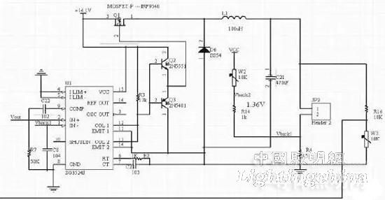
As shown in the figure above, the switching power supply chip dedicated to the switch chip SG3524 generates a 500kHz PWM signal, and the control switch IRF9540 then supplies current to the external circuit through the energy storage original inductor. The output current terminal feeds the resistance voltage back to the SG3524 through the 1K resistor of R14. The feedback input is closed-loop controlled to produce a constant voltage. Then, the 10-bit DA chip TLC5615 is controlled by the MCU to generate the reference voltage input to the 1st pin of the SG3524, that is, the reference voltage input terminal, so that different reference voltages correspond to different output currents. The 2200UF capacitor acts as a filter, and the diode protects the reverse current. The 1K resistor and the 10K precision adjustable resistor form a voltage divider circuit. The output voltage is divided and the sampled voltage is fed back to the feedback input of the input SG3524. The closed loop control PWM makes the output stable voltage. Increasing the PWM latch makes the shutdown more reliable; the comparator (pulse width modulation) output is sent to the PWM latch, which is asserted by the shutdown circuit and reset by the oscillator output time pulse. Thus, when the circuit is turned off, even if the overcurrent signal disappears immediately, the latch can maintain one cycle of off control until the next cycle clock signal resets the latch.
3.4 MCU Control Module
This module consists of the minimum system of the MCU, the LCD module, the independent keyboard and the alarm module. This module can control the current selection and display on the LCD screen through the MCU. When the equivalent DC load resistance is too large, the output voltage limit value is higher than 10.5V and alarm.
Four test results
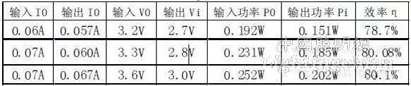
At the beginning of the test results did not meet the requirements, through continuous debugging calculation data, found the circuit
The loss and chip selection are not suitable, which affects the output result. The output can be achieved by replacing the chip and measuring the output. Some of the data is shown in the table below.
Edit: Bober
Best Solar Flood Lights,Solar Motion Flood Lights,Solar Sensor Security Light,Commercial Solar Flood Lights
Jiangmen Liangtu Photoelectric Technology Co., Ltd. , https://www.liangtulight.com