Currently, applications in portable devices are becoming increasingly abundant. With the continuous emergence of various applications such as photo, music, movies, videophone, mobile TV, 3D games, location services, web browsing, email, instant messaging, electronic payment, etc., the data processing capability of portable devices is driven to super The speed of Moore's Law has grown. In high-end portable devices (such as smart phones, hard disk PMP, etc.), there is usually an application processor. These processors provide a platform and power for the ever-changing applications and provide critical product differentiation for device manufacturers. According to the analysis of authoritative market research institutions, the compound annual growth rate (CAGR) of application processors was as high as 48% from 2005 to 2009; by 2009, the sales of application processors in China will reach 3.6 billion.
The Z228 chip of Shanghai Jade Microelectronics Co., Ltd. is a typical application processor with a core voltage of 1.2V, an I/O voltage of 2.5/3.3V, and a package of 441-TFBGA. As can be seen from Figure 1, the appearance of the Z228 chip is slightly smaller than the RMB 5-point coin.
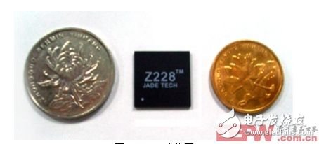
Figure 1: Physical map of the Z228 chip. /I"
You can imagine that the Z228 is an ultra-small notebook motherboard (without DRAM and hard drives, etc.), plus a display, keyboard, mouse, network port and other peripherals, it becomes a pocket notebook. This is a reflection of the concept of system-on-chip (SoC). In fact, the Z228 is a highly integrated SoC chip that combines the high performance, low cost and software flexibility of hardware. The block diagram of the module is shown in Figure 2.
As can be seen from Figure 2, the flexibility of the chip software is mainly reflected by the ARM926EJ core. At present, almost all application processors use the ARM core. In a sense, ARM can be regarded as the de facto standard in the field of portable terminals. Many softwares compatible with the ARM instruction set can be downloaded on the Internet. The high performance and low cost of hardware in the chip is mainly reflected by the MPEG-4 engine and image processing engine. The video codec operation and image processing are implemented in full hardware, which greatly reduces the burden on the ARM core and significantly increases the battery life of the terminal. Another benefit of using a hardware solution is that you don't need to develop it yourself or purchase multimedia codec software from a third party, which shortens the development cycle and reduces development costs.
The technical features and applications of the Z228 chip will be introduced below.
1. ARM926EJ kernel
The Z228 uses the ARM926EJ processor core in the ARM9 series. The core frequency is up to 300MHz in the 0.13um process. Designed for multitasking mobile applications, it combines high performance with low power requirements. With the support of this kernel, the Z228 can smoothly run multimedia applications such as audio, video, images, 2D graphics, Java 3D games.
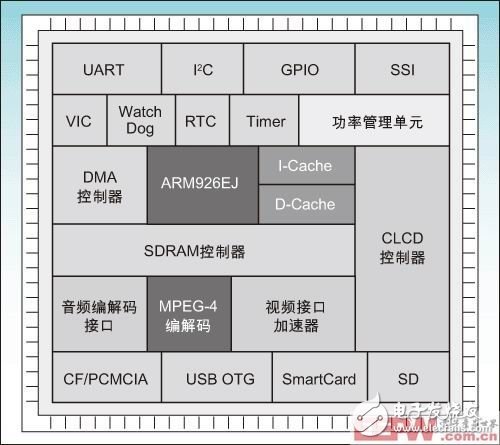
Figure 2: Functional block diagram of the Z228 chip.
The ARM926EJ core in Z228 contains a 16KB instruction cache and a 16KB data cache with a TCM interface. The Memory Management Unit (MMU) supports embedded OS such as WinCE and Linux. The Z228 uses a matrix-based AMBA bus (MAB) to provide sufficient bandwidth for high-throughput data applications. ARM926EJ adopts ARMv5TEJ instruction set, backward compatible with ARMv4 instruction set, and supports popular ARM development and debugging system, which can protect the software investment of terminal equipment manufacturers to the greatest extent.
The Z228 supports ARM's JazelleTM acceleration technology, which greatly increases the speed of Java programs and maintains extremely low power consumption. The MOVE coprocessor increases the efficiency of video coding by more than 50% by implementing the SAD engine.
2. MPEG-4 codec engine
Z228 has built-in MPEG-4/H.263 full hardware codec engine. When performing VGA@30fps full-duplex codec, ARM926EJ has extremely low load (less than 5%), which can smoothly run the operating system and other applications. Compared to the mainstream chips that only support CIF size on the market, the Z228's video performance is more advantageous. When performing real-time decoding with a bit rate of up to 8 Mbps, the picture has no pause. In addition, the high-quality VGA recording has a larger image on the PC than the CIF, and the output to the TV is also better.
Its full hardware implementation makes software interventions minimal and improves product stability. The engine uses patented motion estimation technology and is very power efficient. At VGA@30fps full-duplex codec, the power consumption is less than 120mW.

Figure 3: Decoded image without error protection. Figure 4: Decoded image of Z228.
In order to provide excellent image quality under low bit rate transmission conditions, the engine has video error protection, including strip resynchronizaTIon, data partelling, reversible long encoding (RVLC) and header. The spreading code (HEC), etc., significantly improves the robustness of video transmission in a wireless environment. Comparing Figure 3 with Figure 4, we can show the superior performance of Z228's error-proof technology in improving image quality.
The Z228 also features a high-performance, full-featured video post-processing engine that supports chroma space conversion, arbitrary-scale image scaling, deblocking/de-loop filtering, brightness/contrast/saturation correction, dithering, image masking, and painting. Painting and other functions. The decoded video image is directly processed on the screen after being processed by the engine, and the smooth playback of the video is realized without increasing the power consumption without CPU intervention.
3. Video Interface Acceleration Engine
Z228 built-in video interface acceleration engine, using JD's patented configurable image processing pipeline technology, including EBBI interpolation restore, AWBA white balance adjustment, IBCSA image correction, Gamma color correction, HPFS digital zoom, ADNR denoising, DES edge enhancement, etc. Module. The acceleration engine is connected to the mainstream CMOS/CCD sensor module on the market through a CMOS/CCD image sensor interface circuit, and supports various input formats such as RAW, RGB, and YUV. The Z228 integrates a high-quality JPEG codec module that can handle up to 16 megapixel still images. Electronic framing and on-screen menu functions are also done in hardware.

Figure 5: Software architecture of the Z228 chip.
In addition, the acceleration engine also features CCIR656/601 input and output interface for easy connection to the TV interface, providing popular entertainment applications such as TV recording and TV output.
4. Peripheral interface
As a highly integrated SoC chip, the Z228 has built-in hardware interfaces that not only bring convenience to system developers, but also reduce the cost of the product and reduce the size of the product.
The Z228 supports dual-screen display: 24-bit true color main LCD screen with SVGA (800x600) resolution and a smart LCD module for simultaneous operation as a secondary screen and main screen. The Z228 supports touch screens for easy development of PDAs, learning machines and high-end smartphones.
The Z228 has a built-in USB OTG interface, which makes it easy to communicate with PC mainframes and peripherals, as well as USB storage devices, USB printers or other mobile devices that support the USB protocol.
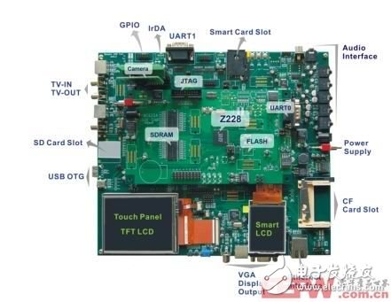
Figure 6: Development board for the Z228 chip.
For mobile devices that require large-capacity memory cards, the Z228 integrates an SD/CF/PCMCIA interface to support expansions up to 4GB.
Z228 also has built-in other peripheral interfaces, which can be used with 2G/2.5G/3G baseband chips, Bluetooth controllers, Ethernet chips, analog audio codecs, TV encoders, infrared transceivers, micro hard disks and other devices. Connected and developed differentiated products.
5. Embedded software
Embedded software plays a very important role in SoC research and development. It embodies product differentiation and acts as a bridge between users and hardware, and is the key to determining the success or failure of a product. The Z228's embedded software uses a layered, flexible architecture, as shown in Figure 5.
The hardware abstraction layer includes board support packages (BSPs), drivers, and diagnostic debugging tools. The BSP consists of a bootloader (bootloader) and a hardware configuration file that provides the software environment at system startup. The hardware abstraction layer logically minimizes the coupling of software and hardware modules, facilitating the accelerated verification of software and hardware and shortening the development cycle. The OS layer provides support for mainstream embedded operating systems such as WinCE 5.0 and Linux 2.6.15. The protocol layer mainly contains the necessary middleware, such as SIP, RTP, RTSP, multimedia library and so on. Several APIs are abstracted by the protocol layer, and the supply layer is called.
From the hardware abstraction layer to the application layer, the Z228 software development kit is formed. It follows modular design principles and is structurally scalable and flexible. For different devices and applications, developers can make the appropriate cuts to strike a balance between cost and performance.
6. Application examples
Based on the Z228 chip, Jade provides a rich interface board and development kit, as shown in Figure 6. Based on this, developers can quickly develop products with different functions.
smart phone. Based on the Z228 chip, developers can quickly develop powerful multimedia smartphones with fewer devices. The Z228 can communicate with the baseband chip via a UART or 68K interface. The Z228 supports mainstream embedded operating systems, supports high-quality audio and video communications, features digital camera/video camera and PDA functions, and has software extension capabilities. The Z228 enables efficient power management and offers a variety of operating modes that extend the battery life of smartphones.
PMP/MP4. Z228's powerful multimedia performance and rich peripheral interface are essential features of the high-end converged PMP. Z228-based PMP can be connected to external hard disk, memory card, camera module, FM module, Bluetooth module, 802.11 module, set photo, video, music, FM radio, recording, TV recording and output, wireless transmission, digital companion, etc. A lot of features in one. The built-in ARM926EJ processor can also run an embedded operating system, supporting Java games, Flash plug-ins, instant messaging software, e-books, etc., fully reflecting the differentiation of PMP products.
Video Surveillance. The Z228 is ideal for building video surveillance systems. Its built-in ARM9 processor and hardware video codec facilitate the development of more flexible and inexpensive distributed terminal equipment and IP-based surveillance networks, in line with the trend of video surveillance to network, digital and intelligent. Z228's advanced video compression algorithm provides good picture quality (greater than 30dB) at lower bandwidths (less than 700kbps); end-to-end delay (excluding transmission delay) is less than 60ms in low-latency mode; ARM9 processor The existence of audio and video synchronization is more convenient.
Facetime. The Z228 can be used to design low cost video telephony and video conferencing systems. Using the Z228, along with a color image sensor module and an LCD display module, the product can transmit bidirectional MPEG-4 video signals. The VGA-size screen, combined with low-latency mode and error-proof technology, significantly improves the user experience. The ARM926EJ processor runs the SIP protocol stack and dynamically adjusts the bit rate of the video stream to accommodate different channel bandwidths.
gree , https://www.greegroups.com