The DC/AC counterflow of fluorescent electronic ballasts almost all adopts the half-bridge circuit topology. For high-intensity discharge lamp electronic ballasts such as high-pressure sodium lamps and metal halide lamps, DC/AC inverters are usually selected. Bridge topology. NBI2037TS single-chip IC from NXP Semiconductors is a new HID lamp full-bridge control and driver, mainly used to drive HID lamps below 100W for general lighting and projectors.
Package and pin function
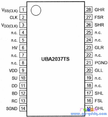
The UBA2037TS is available in an SSOP28 package with pinouts as shown above.
| Pin | symbol | Features |
| 1 | VSS(clk) | Logic oscillator input negative supply voltage |
| 2 | CLK | Oscillator input |
| 3 | VDD(cik) | Logic oscillator input positive supply voltage |
| 4 | n. C. | Not connected |
| 5 | n. C | Not connected |
| 6 | HV | High voltage power input to internal regulator |
| 7 | n. C | Not connected |
| 8 | n. C. | Not connected |
| 9 | VDD | Internal low voltage power supply |
| 10 | SU | Start delay input |
| 11 | DD | Divider failure input |
| 12 | BD | Bridge failure input |
| 13 | RC | Internal oscillator RC input |
| 14 | SGND | Signal address |
| 15 | GHL | Upper left MOSFET gate driver output |
| 16 | FSL | Left floating power supply |
| 17 | SHL | Upper left MOSFET source |
| 18 | n. C. | Not connected |
| 19 | Nc | Not connected |
| 20 | GLL | Below left MOSFET gate driver output |
| twenty one | PGND | Power level |
| twenty two | Nc. | Not connected |
| twenty three | GLR | Below the right MOSFET gate driver output |
| twenty four | n. C. | Not connected |
| 25 | n. C. | Not connected |
| 26 | SHR | Upper right MOSFET source |
| 27 | FSR | Right floating power supply |
| 28 | GHR | Upper right MOSFET gate driver output |
The above table lists the various pin functions of the UBA2037TS.
Basic functions and working principle
Functional Block Diagram UBA2037TS chip integrates a 550V input series regulator, a frequency adjustable oscillator and a selectable divider (÷2), 464V high voltage level shifting circuit, control logic, bootstrap diode, external The clock input circuit and the H-bridge (full-bridge) left high and low end and right high and low (four total) power MOSFET gate drivers, etc., the functional block diagram is shown below.
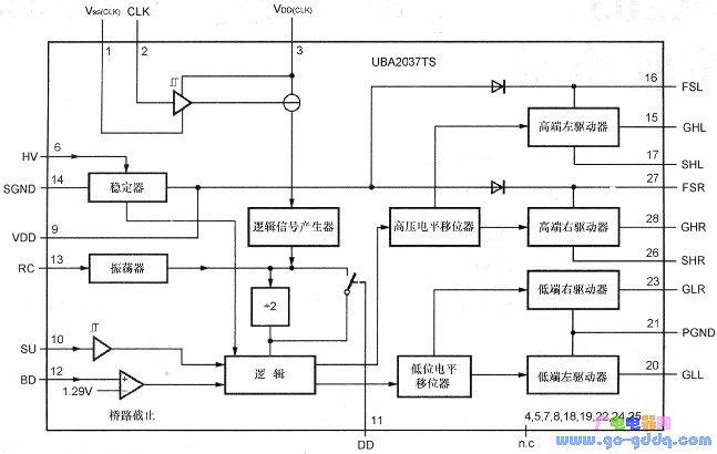
The supply voltage full-bridge DC bus voltage (up to 550V) is applied from the HV pin of the IC (UBA2037TS) to generate DC low to VVDDO for the internal circuit. The low voltage supply can also be applied from the IC pin VDD, in this case, the pin The HV must be connected to pin VDD or pin SGND.
Startup After the IC is powered up, the IC starts when the voltage on pin HV exceeds 13.2V (typ) or the voltage on pin VDD exceeds 9V (typ). During startup, VDD charges the external bootstrap capacitor via the internal bootstrap diode.
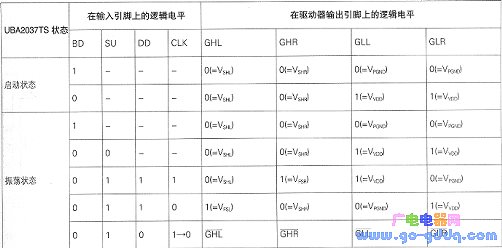
After the oscillator IC is started, the oscillator oscillates and the full-bridge output voltage is dependent on the control signals on the IC pins CLK, SU, DD, and BD, as shown in the following table.
The IC pins VDO(CLK), CLK, and Vss(CLK) can be connected to SGND when the external clock is not being used. In this case, the bridge oscillation frequency fbndge is determined by the resistance Rosc connected between the IC pin RC and VDD and the capacitance Cosc between the pins RC and SGND and the oscillator constant Kosc, and the calculation formula is: fbridge=1/(Kosc ×Rosc×Cosc) At fbridge_500 Hz, Kosc=0.97±0.08.
The external clock signal can be obtained from either the IC pin CLK or the pin RC. In order to obtain a 50% duty cycle of the MOSFET gate drive signal, the clock signal can be divided by 2 via an internal divider (÷2). For this reason, the lC pin DD should be connected to the pin SGND. Non-overlap time In a full-bridge configuration, the non-overlap time is defined as the time interval between the turn-off and turn-on of the other two MOSFETs after the two MOSFETs are turned off, known as the "dead zone". time". The non-overlap time of the UBA2037TS is achieved by an internal adaptive non-overlapping circuit. The shortest non-overlap time is internally fixed at 900 ns.
When the bridge voltage is cut off and the voltage on the IC pin BD exceeds the typical value of 1.29V, all four power MOSFETs in the full bridge are turned off.
The startup delay utilizes a simple RC filter on the IC pin SU (R is connected between pins SU and VDD, C is connected between pins SU and SGND) or can be enabled by a control signal from the processor. delay. The startup delay ensures that the HID lamp system is not activated before the high voltage does not reach a sufficient value.
Application circuit
Offline HID lamp drive solution utilizes AC. Off-line HID lamp electronic ballast circuit powered by mains power supply, usually consisting of EMI input filter, Bridge Rectifier, active power factor correction (PFC) DC-DC boost converter, DC-DC buck converter and The full bridge drive circuit is composed of several parts, as shown in the figure below. In many applications, a DC-DC switching buck converter may not be required. In DC-powered applications (such as automotive), the drive scheme can be greatly simplified, but a DC-DC boost converter is typically required to cascade a full-bridge DC-DC converter. 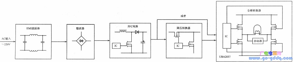
The basic application circuit of the UBA2037TS basic application circuit U-BA2037TS is shown in the figure below. In this HID lamp full-bridge driver circuit, the external clock input, startup delay, and full-bridge-off function are not utilized, so the IC pins CLK, VSS(CLK), VDD(CLK), and pin BD are both grounded (SGND). Since the lC pin DD is grounded, the internal divider is utilized and the bridge commutation frequency is one-half of the internal oscillator frequency. Since Rosc=100kΩ and Cosc=82nF, the full-angle conversion frequency fbndge21/(0.97×100kΩ×82nF) is 125 Hz. Q1 - Q4 is a full bridge switch (MOS-FET). When the output high level signal on pin 28 and pin 20 of UBA2037TS drives Q1 and Q4 to turn on, pin 15 and pin 23 output low, 03 and Q2 are off; when IC pin 15 and pin 23 When the output high level signal drives Q3 and Q2 to turn on, Q1 and 04 are turned off. Therefore, alternating AC current is passed through the HID lamp. The reason why the HID lamp works at low frequency is to avoid the occurrence of acoustic resonance, causing the lamp arc to shake or extinguish the arc, causing damage to the lamp. Select, 100 - 400Hz operating frequency, will produce stroboscopic phenomenon.
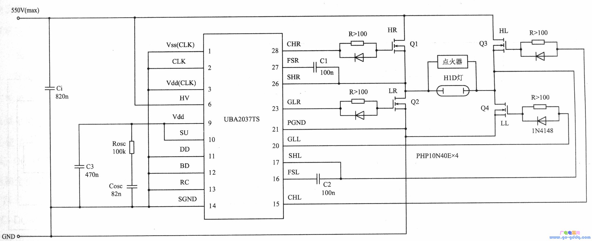
Since the ignition voltage of the HID lamp is 3 to 5 kV, an initiator is required to trigger the HID lamp to illuminate. The HID lamp starter is composed of a semiconductor device with a negative resistance characteristic and a step-up transformer to generate an ignition voltage of several thousand volts.
In the above figure, C1 and C2 are bootstrap capacitors. The MOSFET gate series resistor can make the MOSFET gradually turn on. The diode (1N4148) on the gate connected in parallel with the gate resistor R can accelerate the MOS-FET turn-off.
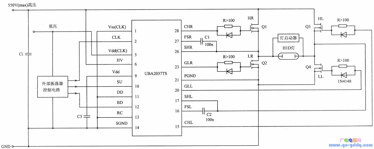
Application Circuit with External Clock Signal When using an external clock signal, the RC pin of the IC should be grounded as shown in the following figure. The IC external oscillator control circuit is used as a system reference. The pin VDD(CLK) is connected to the low-voltage power supply, and the pin is VSS (CLK/ground. If the IC pin DD is connected to VDD, the internal divider is not used: if the pin DD is grounded, The external clock input signal is divided by 2 by an internal divider.
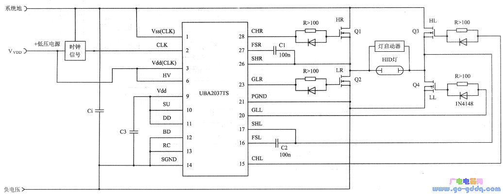
Application Circuit Operating at Negative Voltage When the HID lamp is used as a headlight for an automobile, to limit the mobility of sodium, the full bridge bus of Figures 4 and 5 can be used as a system ground, while in Figures 4 and 5 The ground (SGND/PGND) is added with a negative voltage. In this case, the UDA2037TS pin VDDlCLK) and the pin HV and pin VDD should be connected to the low-voltage power supply VVDD (typically 12V) as shown below.
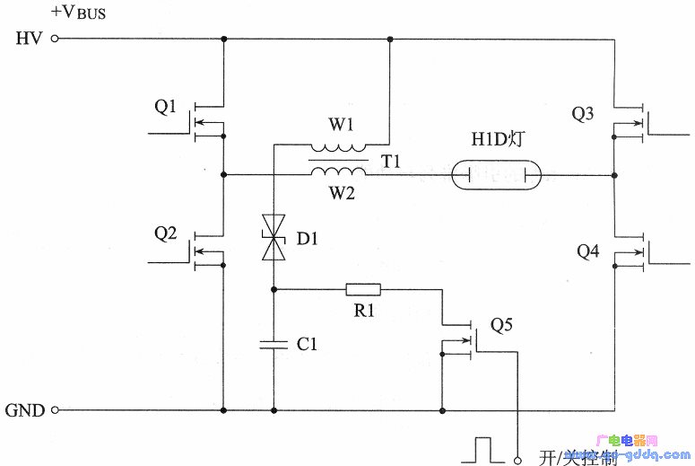
The core component of the starter circuit HID lamp starter is a booster coil, similar to the motorcycle igniter. The following figure shows a schematic diagram of a HID lamp startup circuit. A high-level pulse is applied to the gate of Q5, Q5 is turned on, and the DC high voltage breaks down the bidirectional breakdown diode D1, and the current passes through the primary winding coil W1 of the step-up transformer T1 to generate a 3~ on the secondary boosting winding. The high-voltage pulse of 5kV ignites the HID lamp. Once the lamp is lit, the control signal turns off Q5, and W2 only acts as a ballast.
PTC Thermistor for Overcurrent Protection for Telecom
PTC Thermistor ,Thermistor,Thermistor for Overcurrent Protection ,PTC Thermistor YZPST
YANGZHOU POSITIONING TECH CO., LTD. , https://www.cndingweitech.com