0 Preface
With the growing material wealth of society, security burglary has become a concern of the whole society. The electronic code lock designed based on EDA technology has attracted widespread attention because of its low price, safety, reliability and ease of use. With the field programmable logic device (FPGA) as the design carrier and the hardware description language (VHDE) as the main expression, the Quartus II development software and the GW48EDA development system are designed as electronic design locks, which can realize digital input. Digital clearing, password removal, password change, password lock and password release, etc., therefore, can meet the social security requirements.
1 basic functions of electronic password lock
The main functions of the electronic password lock include:
(1) Digital input: Press a number key, the corresponding number is displayed on the rightmost digital tube, and all the previously entered numbers are shifted to the left by one. The design password is 4 digits, and the system can only display the first 4 digits of the input.
(2) Digital clear: When the clear key is pressed, all the values ​​entered previously are cleared and displayed as “----â€.
(3) Password release: Press the 55# button to release the old password of the electronic password lock.
(4) Password change: After the old password is released, the password can be changed. Enter any four-digit password number and press # to use the entered digit as the new password.
(5) Password lock: After entering the new password, press the 11# button to perform the password lock operation.
(6) Password unlock: press the 99# button, then enter the number; if the input is consistent with the system storage password, the password lock can be turned on; otherwise, it cannot be unlocked.
2 The structure principle of electronic password lock
2.1 The overall structure of the electronic password lock
The overall structure of the electronic code lock is shown in Figure 1. It includes a password lock input module, a control module and a display module. 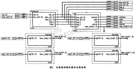
2.2 password lock input module
The circuit block diagram of the code lock input module is shown in Figure 2. It consists of a timing generation circuit, a keyboard scanning circuit, a bounce cancellation circuit, a keyboard decoding circuit, and a key storage circuit. 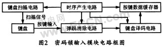
The timing generation circuit is configured to generate working pulse waveforms of three different frequencies in the circuit, including a system clock signal, a bounce cancellation sampling signal, and a keyboard scanning signal.
The keyboard circuit provides a keyboard scan signal. The signal enters the keyboard from ky3 to ky0, and the order of change is 1110-1101-1011-0111-1110... it is repeated. The scan signal 0111 represents a row of buttons that are scanned for *, 0, and #. When the button is pressed, the value read by kx2 to kx0 is 011. The digital relationship of the button positions is listed in Table 1. 
The bounce cancellation circuit prevents misoperations from occurring. Since the matrix keyboard used in the design is a mechanical switch structure, at the moment of switching, a signal bounces back and forth at the contact point. In order for the electronic code lock to work reliably, a bounce cancellation circuit must be added. The bounce elimination circuit uses software delay to eliminate jitter, and its simulation waveform is shown in Figure 3. It can be seen from Fig. 3 that if the sampling signal detects a high level signal twice or more times, the state of the button does change, and the circuit outputs a button signal of one clock cycle; otherwise, it is treated as jitter. Ignore it to eliminate jitter. 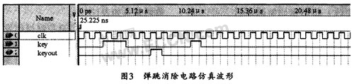
For the keyboard decoding circuit, since the keyboard keys in Fig. 2 are divided into digital keys and function keys, each key can be responsible for different functions, and the output generated by the keyboard (that is, the scan reply signal) cannot be directly used as The code lock controls the input of the circuit, so the keyboard decoding circuit must be used to plan the output form of each button in order to perform the corresponding action.
The keyboard storage circuit can store the new key data generated by each scan, so the new data may overwrite the previous data, so a key storage circuit is needed to record the result of the entire keyboard scan.
Figure 4 shows the simulation waveform of the combination lock input module. In the figure, the numeric key data "0, 1, 2, 3, 4, 5, 6, 7, 8, 9" and the function key data "0100, 0001" The resulting output is different, which proves the correctness of the password lock input module. 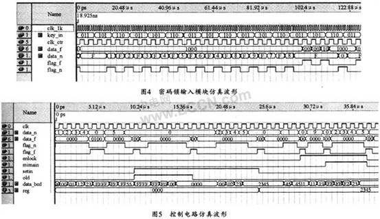
2.3 Control Module
The combination lock control circuit is the control center of the whole circuit, mainly completing the response and control of the digital key input and the function key input. The simulation waveform of the password lock control circuit is shown in Figure 5. As can be seen from Figure 5, the response control process for its numeric key input is as follows:
(1) Press the number key, the first number will be displayed at the far right end of the display, and each time a new number is pressed, the number already existing on the display will be shifted to the left by one digit and will be displayed as a new number. ;
(2) To change the input number, press the * key to clear all entered numbers and re-enter the number.
(3) The electronic code lock is 4 digits. When more than 4 digits are input, the circuit ignores it and does not display the fourth and subsequent digits.
The input response control functions of the function buttons are as follows:
(1) Clear function: Press the * key to clear all the entered numbers and display it as “----â€.
(2) Change the password: Press the 55# button, enter the old password (“0000†in the design), and press the # button to release the old password. Then enter 4 digits, then press #, you can use 4 digits as the new password.
(3) Password lock: After entering the new 4-digit password number, press the 11# key to lock the password.
(4) Password unlock: press the ## key to enter the password to unlock. If you enter the password of “2345†and then press the # key, the system will compare the digital input of the keyboard with the number in the register. If they are consistent, they will be given. An unlock signal, the password lock is unlocked; otherwise the password input is invalid.
2.4 display module
The display module of the electronic code lock is relatively simple, and its function is to convert the BCD code output of the control module into a 7-segment display code, and then drive the digital tube, and the simulation waveform thereof is as shown in FIG. 6. 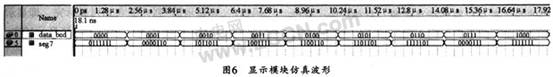
3 Integration and verification of electronic password locks
To complete the design of the electronic combination lock, the above three functional modules must also be integrated. Its integrated circuit diagram is shown in Figure 1.
This design selects the GW48EDA system produced by Hangzhou Kangxin Electronics Co., Ltd. as the hardware verification system, and selects EP1K30TC144-3 of Altera Company as the main control chip. The chip is a field-programmable logic device based on look-up table structure. Its basic logic unit is a programmable look-up table, which can realize combinational logic operations and can implement sequential logic operations with programmable registers. The design only needs to lock the input and output pins in the overall design of the electronic code lock, and then recompile and download, then the hardware verification of the electronic code lock can be performed. Experiments show that this design can realize all the functions of electronic password lock.
4 Conclusion
In this paper, the field programmable logic device (FPGA) is used as the design carrier, and the hardware description language (VHDL) is the main expression. The QuartusII development software and the GW48EDA development system are used as design tools to design a password input, digital clear, and password relief. Electronic password lock for functions such as password setting and password activation. At the same time, the working principle and hardware and software implementation methods of the electronic password lock are explained. The timing simulation and hardware verification of the electronic code lock show that the circuit can achieve the required functions. Because the FPGA chip in this design is small in size, low in power consumption, cheap in price, safe and reliable, the number of passwords can be changed with a little modification, and it is convenient to maintain and upgrade, and it is easy to make an ASIC chip, so it has better Application prospects.
This article refers to the address: http://
42mm DC Brushless Gear Motor mainly including 42RPBL4250 and 42RPBL4260

Since spur gearbox or worm gearbox has a limited lifespan, and brushless motor can achieve more than 2000 continuous hours, so we merely use dc brushless motor with spur gearbox.
42RPBL4250 and 42RPBL4260 are both DC Planetary Gear Motor, the available gear ratio including: 3.7, 5, 13, 18, 25, 49, 67, 92, 125, 181, 246 etc
Brushless motors are typically 85-90% efficient whereas brushed DC motors are around 75-80% efficient. This difference in efficiency means that more of the total power used by the motor is being turned into rotational force and less is being lost as heat.
Brushless DC motors have many advantages over their brushed DC motor counter parts. The most obvious advantage of a brushless motor is its lack of brushes and physical commutator. This difference means that there are many fewer parts that can wear out or break and need to be replaced than in a brushed motor.
42mm DC Brushless Gear Motor
42Mm Brushless Dc Gear Motor,42Mm Brushless Gear Motor,42Mm Brushless Electric Motor,42Mm Brushless Motor Controller
SHENZHEN DONGMING MOTOR CO., LTD. , http://www.dongminggp.com