1 Introduction
This article refers to the address: http://
The multi-output military vehicle power supply mentioned in this paper is a dual DC/DC switching power supply with low input and output voltages and low current. The input voltage is 9~15V, and the output voltage is 2 channels: 24V all the way; 5V all the way. The 24V output is simultaneously supplied with three loads; the input voltage is directly supplied to the two loads, as shown in Figure 1.
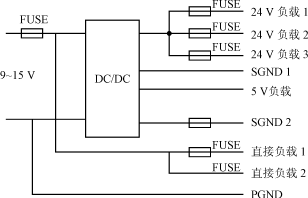
Figure 1 circuit block diagram
Taking into account the requirements of independent output protection, the power supply adopts two independent circuit structures. The output power of 24V is larger, and the output power of 5V is smaller.
Here are some introductions to some of the special designs in the circuit.
2 radiator design
The heat dissipation method is the first part to be considered in the design of the power supply product, because it is related to the selection of components in the circuit design, the design of the PCB, and the like. The usual power products are cooled by fans, which can achieve better heat dissipation.
The military vehicle power supply mentioned in this paper, due to long-term operation in the environment of vibration and shock, the use of fan cooling will affect the reliability of the power system. Therefore, the natural cooling structure is adopted. The structure of the heat sink of the whole device is shown in Figure 2. The power semiconductor device is placed on the back side of the PCB and adheres to the bottom plate, and is directly radiated through the bottom plate. The bottom plate is made of thick aluminum material, and the whole device is mounted on a large iron plate (armored vehicle). Both sides of the device use winged fins to serve as a support. In this way, the arrangement of the entire heat sink can not only achieve better heat dissipation effect, but also make full use of the space of the PCB board, thereby reducing the volume of the entire device to some extent.
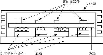
Figure 2 heat sink structure
3 triple overcurrent protection
Because it is a military vehicle power supply, the stability and reliability requirements of the device are very high. Therefore, triple overcurrent protection, that is, microsecond protection, millisecond protection, and second protection are adopted.
3.1 microsecond protection
Microsecond protection means that when the power supply has an output overcurrent or short circuit, it can be protected in one switching cycle. Because the switching cycle is usually designed in microseconds, this protection is called microsecond protection. The specific implementation method is shown in Figure 3. The peak current control signal is connected to the pin ISE of the PWM chip L5991 [1] . When the voltage of the foot ISE is greater than 1V, the output of the L5991 is low, thereby turning off the switch. This protection is judged at each switching cycle, so the reaction speed is faster to protect the transient overcurrent.
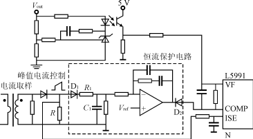
Figure 3 Current peak protection and constant current protection circuit
3.2 millisecond protection
The millisecond protection refers to the constant current protection of the PI ring. Its protection time is usually in the range of tens to hundreds of switching cycles, which is called millisecond protection here. Since the peak protection of the sampling current is one-cycle protection, the stability is not very good and can only effectively protect the overcurrent of the transition process. Therefore, for short-circuit or overcurrent for a long time, it is necessary to use the constant current protection of the PI ring here. In the dotted line of Figure 3, the constant current protection circuit uses the current signal in the peak current control as the input signal, and obtains a peak hold circuit composed of D 1 , R 1 , C 1 and a PI link composed of the operational amplifier. The error signal, when the output current of the converter exceeds a limit value, controls the duty cycle of the PWM chip, thereby maintaining the output current at a limited value. Due to the presence of D 2 , when the output current is lower than the current limit value, the control of the duty cycle of this part of the circuit does not work.
3.3 second level protection
The second-level protection refers to the self-recovery fuse protection in the circuit (the protection time of the self-recovery fuse is more than a few seconds), as shown in Figure 1. When the circuit is in the above-mentioned constant current protection, if the time is too long, the device will overheat. If the heat design is done according to the overcurrent protection, the cost of the device will increase. Therefore, for short-circuit or over-current for a long time (more than a few seconds), it is necessary to protect with a fuse. The self-recovery fuse is used in this device. When the load returns to normal, the self-recovery fuse can return to the normal conduction state. Another reason for using a self-recovering fuse is that each load required by the device is independently protected. When one-way overcurrent protection is applied, the self-recovery fuse of the circuit is disconnected, and the other circuits can still work normally. The 5V that does not have a self-recovery fuse is considered to have only one load, which can be protected by microseconds and milliseconds. In addition, since the 5V output voltage is relatively small, the self-recovery fuse will affect its output adjustment rate.
4 RCD/RC double absorption
Because of the leakage inductance of the transformer, the flyback converter will generate a relatively high voltage spike at both ends of the D-S of the switch when the switch is turned off. This voltage spike increases the voltage stress of the switching transistor and at the same time generates electromagnetic interference, so it must be suppressed by an absorbing circuit. The RCD snubber circuit is relatively common in low power applications due to its simplicity and ease of implementation. The RCD absorption flyback converter is shown in Figure 4. It can be seen from Fig. 6 that after the RCD absorption circuit is added, the voltage spikes across the switch tube D-S are greatly reduced, but at the same time, a new higher frequency oscillation is also generated, which is due to the leakage of the primary side of the transformer. The sense is caused by the resonance of the junction capacitance of the diode. This oscillation must be suppressed from the viewpoint of electromagnetic compatibility. Changing the parameters of R , C , and D has little effect on the new oscillation. Therefore, it is necessary to add other circuits to suppress. Adding the RC absorption circuit at both ends of the switch tube D-S has achieved ideal results in the experiment. Figure 5 shows the RCD/RC dual absorption circuit. Figure 7 shows the experimental waveforms of the RCD absorption flyback converter and the RCD/RC double absorption flyback converter switching transistor V ds .
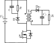
Figure 4 RCD absorption circuit
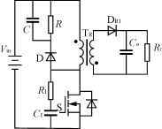
Figure 5 RCD / RC double absorption circuit
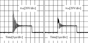
(a) Without snubber (b) RCD snubber
Figure 6 Experimental waveform of v ds before and after RCD absorption circuit

(a) RCD snubber (b)RCD/RC snubber
Figure 7 Experimental waveform of v ds after adding RCD absorption circuit and RCD/RC double absorption circuit
5 resonant RCD reset
Forward converters have a variety of reset modes: resonant reset; third winding reset; RCD reset; active clamp. Here is a low-cost compromise solution: resonant RCD reset.
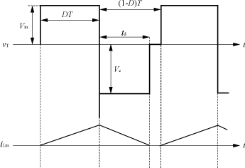
As shown in Fig. 8(a), the resonant reset forward converter has a capacitor C connected in parallel with the main switch S, and a sine wave is generated by the capacitor C and the transformer magnetizing inductance L m to reset the transformer. Figure 8(b) is the main operating waveform of the resonant reset forward converter, where V T is the voltage across the transformer and i L m is the excitation current of the transformer. These waveforms take into account the presence of transformer leakage inductance and are waveforms under heavy loads. The resonant reset voltage should be a sine wave if the leakage inductance is not considered or the load current is zero. When the switch is turned off, there is a voltage spike on the transformer, which is caused by the transfer of the energy stored in the leakage inductance L s to the resonant capacitor C , which is the leakage inductance of the transformer and the resonance of the capacitor C. This resonance period is much smaller than the resonance period of the magnetizing inductance and the capacitance C.
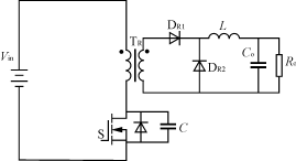
(a) Resonant reset forward converter

(b) Resonant reset forward converter operating waveform
Figure 8 Resonant reset forward conversion circuit and working waveform
Figure 9 (a) shows the RCD reset forward converter, that is, a diode D, capacitor C , and resistor R are connected in parallel on the transformer, and the inductor is induced by the magnetizing inductance and leakage inductance when the switch S is turned off. The potential causes diode D to conduct and the voltage on capacitor C resets the transformer. Figure 9(b) shows the main operating waveform of the RCD reset forward converter. The voltage across capacitor C is approximately DC voltage during one switching cycle, and the RCD reset voltage is a square wave. Similarly, when the switch is turned off, there is a voltage spike on the transformer, which is caused by the leakage inductance of the transformer and the resonance of the junction junction capacitance.
(a) RCD reset forward converter
(b) RCD reset forward converter operating waveform
Figure 9 RCD reset forward converter circuit and working waveform
Both resonant reset and RCD reset have their own advantages and disadvantages, and the advantages and disadvantages of the two reset methods are basically complementary.
1) According to the volt-second balance principle, the average value of V T in one cycle should be equal to zero. The reset voltage of the resonant reset is a sine wave, so the platform of the reset voltage is relatively high, that is, the V DS voltage platform of the switch S is relatively high, and the reset voltage of the RCD reset is a square wave, so the platform for resetting the voltage is relatively low, That is, the V DS voltage platform of the switch S is relatively low.
2) Resonant reset The voltage spike on the forward converter transformer (which is ultimately reflected in the voltage spike of v DS ) is caused by the transformer leakage inductance L S and capacitor C resonance, and the voltage spike on the RCD reset forward converter transformer is It is caused by the leakage inductance L S of the transformer and the junction capacitance of the switch S. Since the capacity of the capacitor C is much larger than the junction capacitance of the switching transistor S, the resonance period of the resonance reset voltage spike is much larger than the resonance period of the RCD reset voltage spike, and therefore, the load current energy on the transformer leakage inductance L S is constant. The voltage peak amplitude of the resonant reset is much lower than the voltage spike of the RCD reset. From another point of view, it can be considered that the capacitance C of the resonant reset forward converter connected in parallel between the switching tubes D-S functions to absorb voltage spikes.
3) The excitation energy and the leakage inductance energy of the RCD reset forward converter are all consumed on the resistor R , and the excitation energy and the leakage inductance energy of the resonance reset forward converter are substantially not consumed, as shown in Fig. 8(b). However, since the resonant reset forward converter is turned on before the switch is turned on, the voltage across the capacitor C is V in , so there is ![]() The energy consumption of CV in 2 is during the opening of the switch.
The energy consumption of CV in 2 is during the opening of the switch.
4) It can be seen from the waveforms of i L m in Fig. 8(b) and Fig. 9(b) that the magnetic bias of the transformer of the resonant reset forward converter is relatively small, and the magnetic bias of the transformer of the RCD reset forward converter is large.
The above analysis can be known that the forward converters of the two reset modes have their own advantages, but the disadvantages are also obvious, and in some cases, there are large bottlenecks in design. It is not difficult to combine the two reset methods to soften their respective shortcomings, but also bring a new advantage, that is, the resonant RCD reset forward converter.
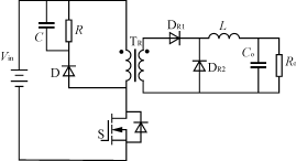
Figure 10 (a) shows the resonant RCD reset forward converter, which can be seen on the line is the combination of the resonant reset forward converter and the RCD reset forward converter. Figure 10 (b) is the main operating waveform of the resonant RCD reset forward converter. The resonant RCD reset forward converter can be divided into five stages in one cycle.
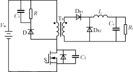
(a) Resonant RCD reset forward converter
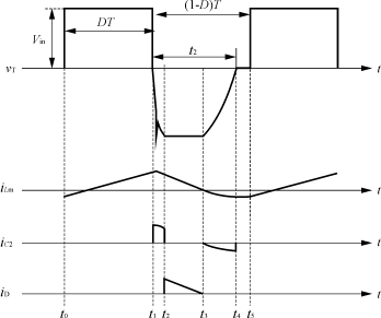
(b) Resonant reset RCD forward converter operating waveform
Figure 10 Resonant RCD reset forward converter circuit and working waveform
(1) Stage 1 [ t 0 ~ t 1 ] At time t 0, the main switch S is turned on, the input voltage is applied to the transformer, and the excitation current linearly rises. The secondary side diode D R1 is turned on.
(2) Stage 2 [ t 1 ~ t 2 ] t 1 At time S is turned off, the first thing that occurs is the resonance reset, and the stored energy on the leakage inductance is transferred to the capacitor C 2 to generate a voltage spike (this is the leakage inductance and capacitance C). 2 resonance). Then leakage inductance and magnetizing inductance and capacitance C 2 together resonance. Since the voltage on the transformer is positive and negative, the secondary rectifier diode D R1 is turned off, and the freewheeling diode D R2 is turned on.
(3) Stage 3 [ t 2 ~ t 3 ] When the reset voltage resonates to exceed the voltage on C 1 , the diode D is turned on, and the exciting current flows to the capacitor C 1 . It becomes the state of RCD reset. At this time, the exciting current linearly decreases. This also ensures that the reset voltage is not too high, so that the voltage stress of the switching transistor is controlled. When the excitation current drops to zero, the state ends.
(4) Stage 4 [ t 3 ~ t 4 ] After the excitation current drops to zero, the diode D is turned off. However, the energy on C 2 is fed back to the magnetizing inductance, that is, at this time, C 2 and the magnetizing inductance resonate. The voltage on C 2 drops and the excitation current increases in reverse. Until the voltage on C 2 drops to equal the input voltage, that is, the voltage on the transformer drops to zero, and the state ends.
(5) Stage 5 [ t 4 ~ t 5 ] As long as a slight up-down and negative-down value appears on the voltage on the transformer, the secondary diode D R1 is turned on and the exciting current flows through D R1 . However, this current is not sufficient to provide the load current, so the freewheeling tube D R2 also continues to conduct, providing an insufficient portion of the load current. At the same time, the common conduction of D R1 and D R2 also ensures that the voltage on the transformer is zero and the excitation current remains unchanged. This state is maintained until the switch S is again turned on.
The value of the resonant capacitor C 2 of the resonant RCD reset forward converter should be smaller than the resonant capacitor C of the resonant reset forward converter, so that the rise and fall of the reset voltage is faster in the resonant reset phase (phase 2 and phase 4), so In the same case that the reset is completed within t 2 time, the resonant RCD reset forward converter has a lower platform voltage than the resonant reset, and is close to the platform voltage of the RCD reset forward converter. Since C 2 is smaller than C , it is much larger than the junction capacitance of the switching transistor. Therefore, the voltage peak of the resonant RCD reset forward converter transformer is slightly larger than the resonant reset, and much smaller than the RCD reset. From the above analysis, the resonant RCD reset forward converter transformer has a lower voltage platform and peaks, and therefore, the switching stress is lower. In the case of excitation energy loss (partial excitation energy feedback), switching loss ( C 2 < C ), transformer magnetic bias (see the excitation current waveform of various reset modes), the resonant RCD reset forward converter is a resonant reset positive The tradeoff between the converter and the RCD reset forward converter.
6 Application of saturated inductor
Since the power supply unit is a low-voltage, high-current input and output, the reverse recovery problem on the diode is quite serious, especially the freewheeling diode D R2 of the forward converter. Fig. 11(a) shows the voltage waveform on D R2 of the forward converter, and it can be seen that there is a high voltage spike. This not only increases the losses, raises the rated voltage of the required device, but is also very disadvantageous for electromagnetic compatibility. The use of a saturating inductor in series with the diode, as shown in Figure 11(b), can greatly reduce the reverse recovery of the diode without adding much loss. After adding a saturated inductor, the voltage waveform on the diode D R2 is as shown in Figure 11(b). It can be seen that after adding a saturated inductor, the voltage spike on D R2 drops from nearly 160V to 80V.
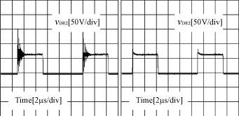
(a) without saturation inductor (b) plus saturation inductor
Figure 11 Voltage waveform across DR2 before and after saturation inductor
7 Conclusion
This paper describes the design of the very demanding military vehicle power supply and the solutions to some special problems in the experimental process, and also put forward some novel ideas. These views have certain reference for future switching power supply design.
Quickly brew the perfect cup of tea or make pour over coffee right at the table with the Electric Tea Kettle. With 1500 watts, this Electric Kettle boils water faster than a microwave, and is safer to use than a stovetop kettle because it automatically turns off when the water reaches a boil. Serving at the table is no problem as the kettle lifts off the base without the cord. Additional features include two water level windows and a pull-lid to make filling and serving easy.
Features:
- Thermostat Control – Having a thermostat control allows the kettle to [know" when to shut off. This will prevent damage to the heating element and is an important feature in all modern styles.
- Auto shut off/Boil Dry Protection/Fuse – these are three features that are great for protecting the safety of users as well as extending the life of the electric kettle. The fuse and boil dry protection shut the kettle off if the water gets down below a certain level or if it`s left on for an extended period of time, It doesn`t burn up the kettle.
- Colors and Designs – Electric kettles come in all shapes, sizes and colors. Finding one that will fit with the kitchen design is actually pretty easy. Finding one that matches and that has the features you`re looking for can be a bit harder, but with all the choices available and the newer models on the market today, you will be able to find the perfect electric kettle for your kitchen.
- Savety in Electric- the heating element is typically fully enclosed, with a power rating of 2–3 kW at 220V. In countries with 110V mains electricity, kettles may be less powerful (1–1.5 kW) to avoid drawing too much current and requiring a very thick supply wire.
Application:
Heat the tea thoroughly
Bottle the water/beer
Boil water
Electric Tea Kettle
Electric Tea Kettle,Stainless Steel Electric Tea Kettle,Cordless Electric Tea Kettle,Electric Cordless Glass Tea Kettle
Guangzhou Taipeng Electrical Appliances Technology CO., LTD. , http://www.kettles.pl