
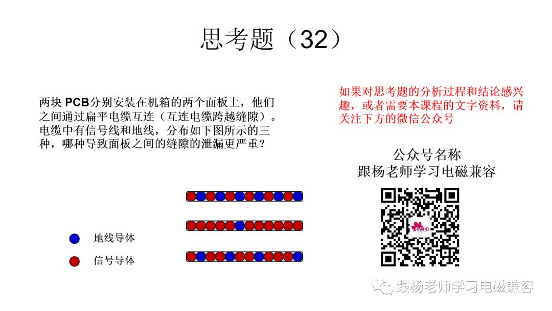
Prep questions
When you design the product, the signal ground on the PCB is connected to the metal chassis. What do you decide how to connect them?
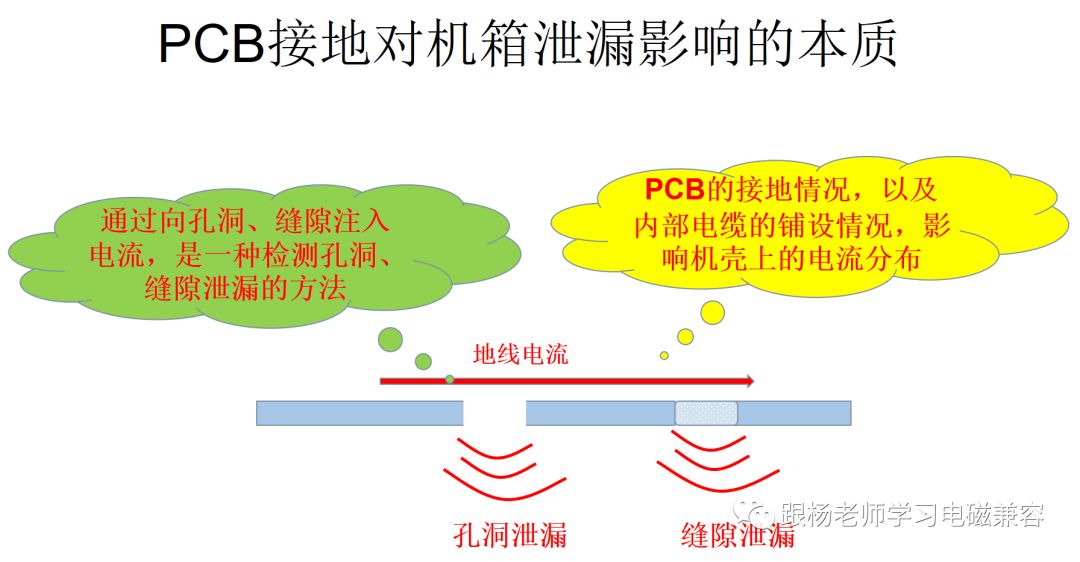
The reason why the signal ground of the PCB board is connected with the shielding chassis may affect the electromagnetic shielding effectiveness of the chassis, mainly because the signal ground current on the PCB board is shunted to the metal chassis panel.
If there is a conductive discontinuity such as a hole or gap in the metal chassis, electromagnetic radiation will occur at these locations. This principle is the same as the electromagnetic leakage of holes and gaps, except that the current on the panel surface is induced by the electromagnetic field. This is directly injected by the PCB.
In the construction of the shielded room, electromagnetic leakage occurs if the weld between the two metal plates is not welded. Therefore, after the shielding room is completed, each weld seam needs to be inspected before the exterior decoration.
One method is to inject an alternating current from a diagonal position on a certain surface (eg, the top surface) of a shielded room, and then use an electromagnetic field leak detector to detect the leak along the weld line. Where the leakage electromagnetic field can be detected, where the weld is There may be a problem.
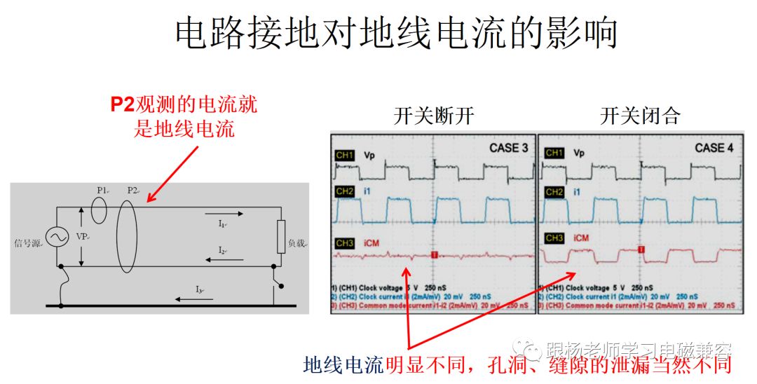
We use this experiment to observe the condition of the ground current.
This experimental device is not unfamiliar to us and was seen during the study of common-mode currents.
The left figure is the experimental device. The ground of a circuit passes through one point, or two points are connected to the panel of the metal chassis. We observe the current flowing through the metal panel of the chassis.
There are two current probes on the circuit, where P2 detects the current flowing through the metal chassis panel.
The two graphs on the right are the current waveform (lowest red waveform) flowing through the metal chassis panel when the circuit is grounded (switch disconnected) and grounded (switch closed).
It can be seen that the waveform of the current is completely different depending on the grounding state. Therefore, the panel has holes, gaps, etc. Their electromagnetic radiation is certainly different.

We further analyze the relationship between PCB grounding and chassis leakage.
The mechanism of the influence of the PCB ground state on the electromagnetic leakage of the chassis was discussed earlier because a part of the ground current is shunted to the metal chassis panel.
What are the factors related to this diversion effect? If we understand the factors that affect the current shunt, we can control these factors to reduce the current diverted to the chassis, thereby reducing leakage.
In the figure, the ratio of the current I2 to the current I3 depends on the ratio between the impedance of the I1-I2 loop and the impedance of the I1-I3 loop. If the impedance of the I1-I2 loop is much smaller than the impedance of the I1-I3 loop, the current I3 can be very small.
In order to reduce the impedance of the I1-I2 loop, we should minimize the area of ​​the I1-I2 loop. In the foregoing, we have discussed the importance of the control loop area for reducing differential mode radiation. Here again, we can see that the control circuit area can reduce the flow of the ground current to the chassis panel.
In addition, when the current I2 flows through the ground on the PCB, it will form a voltage V, which also generates current on the chassis panel, which is also a source of leakage. Therefore, it is also very important to minimize the impedance of the PCXB board ground.
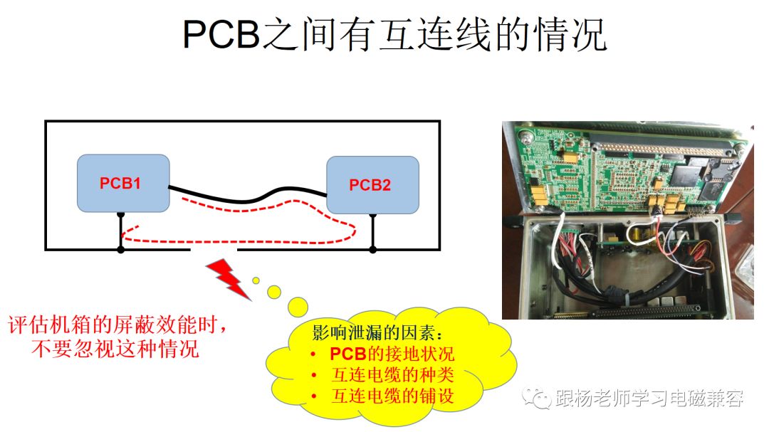
We extend the case of the front single PCB to the case of two PCB interconnections.
As shown on the left. The two PCBs are interconnected by a single cable, and the signal grounds on both PCBs are connected to the panel of the metal chassis.
What happens at this time is similar to that of a single PCB, but it is often more serious.
On the one hand, since the loop area of ​​the signal line in the cable is often larger than the signal loop area on the circuit board, it has a higher impedance, which will cause more current to be shunted to the chassis panel.
On the other hand, there is often more common-mode current on the interconnect leads, and these common-mode currents also pass through the chassis panel.
Therefore, when we lay the cables inside the chassis, we must avoid the cables passing through holes and gaps, which can cause serious leakage.
The figure on the right shows the actual case of an internal cable in the chassis. It can be seen that a large number of cables cross the gap. This chassis will cause more serious electromagnetic leakage.
In front, we analyzed the impact of the PCB ground state on the chassis leakage from the perspective of the metal chassis current shunting the PCB ground current.
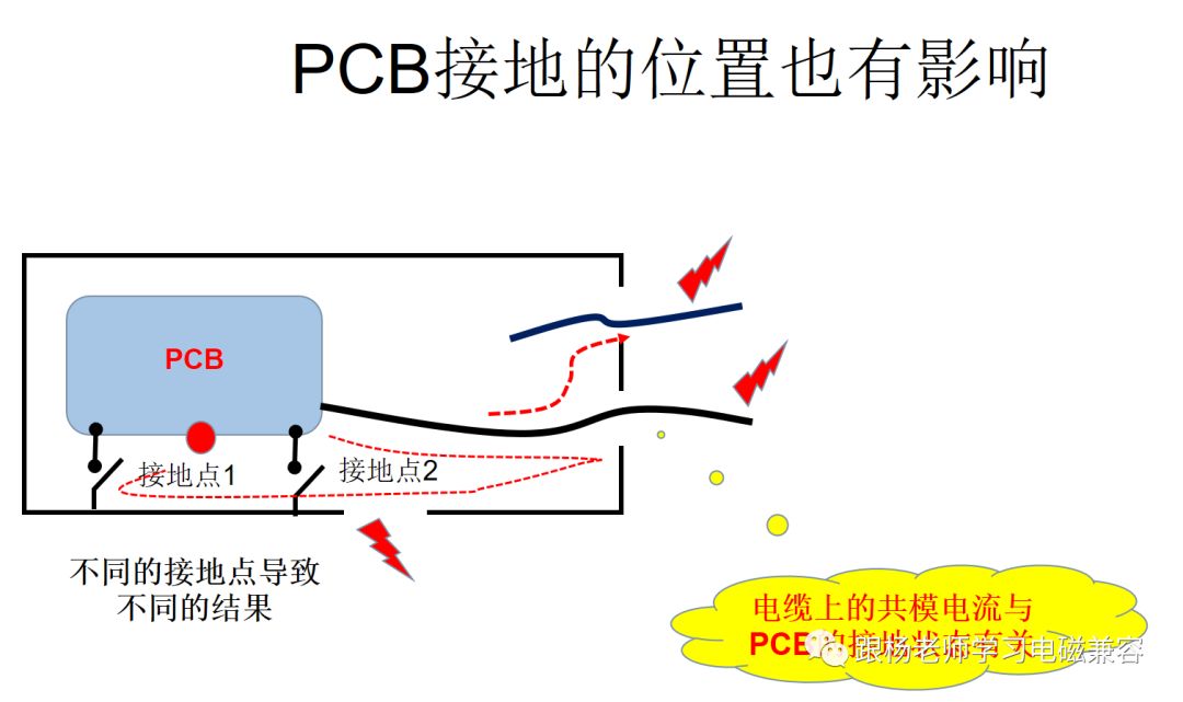
The PCB grounding position will also have a certain impact on the chassis leakage. Details are as follows.
As shown in the figure, a cable is dragged on the top and bottom of a PCB. The cable runs through the chassis.
It can be seen that there are two locations on the PCB that can be grounded, one is ground point 1 and the other is ground point 2. Due to the ground noise voltage on the PCB board, when the PCB is grounded at the grounding point 1, the common mode current on the cable will be larger than when the grounding point 2 is grounded, and therefore, the resulting electromagnetic leakage is also greater.
Common-mode currents on the cable can cause three electromagnetic leaks.
First, as shown in the figure, the common mode current on the cable forms a loop through the panel. If there are holes or gaps in the panel, leakage occurs.
Second, the cable passes through the chassis panel and generates radiated emissions.
Thirdly, next to this cable, there is another cable that passes through the chassis panel. Due to the space coupling effect, the other cable also generates stronger radiation. As shown in the figure on the right, there are often many cables on one panel.
Please remember that a PCB design rule is that the PCB should be set at the ground point where the I/O cable is connected.

Randm Vape,Randm Tornado Vape,China Randm Tornado Vape,Randm Tornado Disposable,Randm Disposable Vape Manufacturer
Nanning Nuoxin Technology Co., LTD , https://www.nx-vapes.com