Author: Texas Instruments Errol Leon, Richard Barthel, Tamara Alani
introduction
Zero-drift amplifiers use unique self-correcting technology to provide ultra-low input offset voltage (Vos) and near-zero input offset voltage drift over time and temperature (dVos/dT) for general and precision applications. TI's zero-drift topology also provides other advantages, including no 1/f noise, low broadband noise and low distortion-simplifying development complexity and reducing costs. This can be done in one of two ways; chopper or auto zero. This technical note will explain the difference between standard continuous-time and zero-drift amplifiers.
Suitable for zero-drift amplifier applications
Zero-drift amplifiers are suitable for a variety of general and precision applications, allowing them to benefit from the stability of the signal path. The excellent offset and drift performance of these amplifiers makes them particularly useful early in the signal path, where high-gain configurations and interfaces to connect microvolt signals are common. Common applications that benefit from this technology also include precision strain gauges and weight scales, current shunt measurements, thermocouples, thermopiles, and bridge sensor interfaces.
Rail-to-rail zero-drift amplifier
System performance can be optimized by using standard continuous-time amplifiers and system-level automatic calibration mechanisms. However, this additional automatic calibration requires complex hardware and software, which increases development time, cost, and board space. Another more effective solution is to use zero-drift amplifiers, such as OPA388.
The traditional rail-to-rail input CMOS architecture has two differential pairs; one PMOS transistor pair (blue) and one NMOS transistor pair (red). Zero-drift amplifiers with rail-to-rail input operation use the same complementary p-channel (blue) and n-channel (red) input configurations shown in Figure 1.
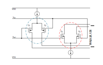
Figure 1. Simplified PMOS/NMOS differential pair
The result of this input architecture exhibits a certain degree of crossover distortion (for more information on crossover distortion, see Zero Crossover Amplifier: Features and Benefits). However, the offset of the amplifier will be corrected by its internal regular calibration, so the amplitude of the offset change and crossover distortion are greatly reduced. Figure 2 shows a comparison of offset between standard CMOS rail-to-rail and zero-drift amplifiers.
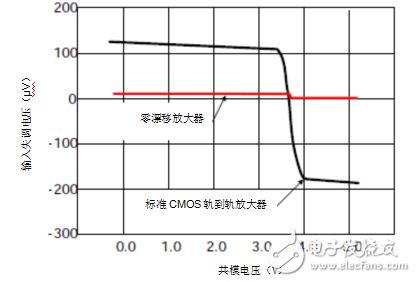
Figure 2. Comparison of CMOS and zero-drift input offset voltages
How zero drift works
The internal structure of a chopping zero-drift amplifier can have as many stages as a continuous-time amplifier—the main difference is that the input and output of the first stage have a set of switches for inverting the input signal during each calibration cycle. Figure 3 shows the first half of the cycle. In the first half of the cycle, both sets of switches are configured to flip the input signal twice, but the offset flips once. This keeps the input signal in phase, but the polarity of the offset error is reversed.
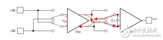
Figure 3. The first half of the internal structure
Figure 4 shows the second half of the cycle. Here, both sets of switches are configured to pass signals and offset errors in an unaltered manner. In fact, the input signal never changes in phase, and remains unchanged. Since the offset errors from the first clock phase and the second clock phase have opposite polarities, the errors are averaged to zero.
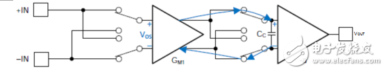
Figure 4. The second half of the internal structure
Use a synchronous notch filter at the same switching frequency to attenuate any residual errors. This principle is still valid throughout the input, output and environmental operation of the amplifier. Essentially, TI's zero-drift technology provides ultra-high performance and excellent accuracy with this self-correcting mechanism.
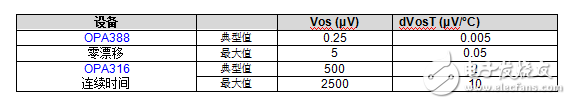
Table 1 shows the comparison between Vos and dVos/dT of continuous-time and zero-drift amplifiers. Note that the Vos and dVos/dT of the zero-drift amplifier are three orders of magnitude smaller.
Auto-zeroing requires different topologies, but the functions are similar. Auto-zeroing technology has less distortion at the output. Chopping makes broadband noise lower.
Noise in zero-drift amplifiers
Generally, zero-drift amplifiers have the lowest 1/f noise (0.1 Hz-10 Hz). 1/f noise (also known as flicker or pink noise) is the main source of low-frequency noise and can be harmful to precision DC applications. Zero-drift technology uses a periodic self-correction mechanism to effectively offset slowly changing offset errors (such as temperature drift and low-frequency noise).
Figure 5 shows the 1/f and broadband voltage noise spectral density of zero-drift (red) and continuous-time (black) amplifiers. Note that the zero drift curve has no 1/f voltage noise.
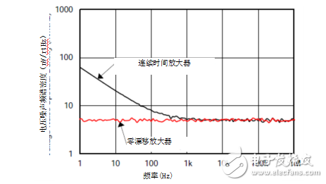
Figure 5. Voltage noise comparison
Again, why choose a zero-drift amplifier?
Zero-drift amplifiers can provide ultra-low input offset voltage, near-zero input offset voltage drift over temperature and time, and no 1/f voltage noise—these design factors are critical for general and precision applications.
Other resources
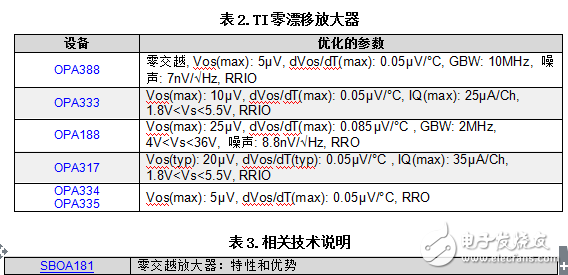
Table 2 below highlights some of TI's zero-drift amplifiers. For a complete list, click to view the results of Texas Instruments’ parametric search tool.
Delivery from European Warehouse
Guangzhou Fengjiu New Energy Technology Co.,Ltd , http://www.flashfishbatteries.com