Lithography is the most important processing technology for integrated circuits. His role is similar to that of lathes in metalworking workshops. In the entire chip manufacturing process, the implementation of almost every process is inseparable from the lithography technology. Lithography is also the most critical technology for manufacturing chips. He accounts for more than 35% of the chip manufacturing cost. In today's technological and social development, the growth of lithography technology is directly related to high-tech fields such as the operation of mainframe computers.
Lithography technology is closely related to our lives. We use mobile phones, computers and other various electronic products. The chips inside can not be separated from the light technology. The world today is an information society, and all kinds of information flows in the world. The photolithography technology is to ensure the manufacture of information-carrying carriers. Has an irreplaceable role in society.
Principles of lithography
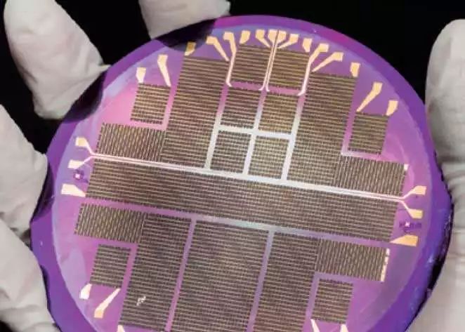
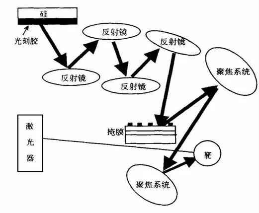
Lithography is to make the circuits and functional areas required for chip production. The light emitted by the photolithography machine is used to expose the photoresist-coated sheet through a photomask with a pattern, and the photoresist will change in properties after being exposed to light, so that the pattern on the photomask is copied onto the sheet, so that the sheet has an electronic circuit The role of the graph. This is the role of lithography, similar to camera photography. The photo taken by the camera is printed on the film, and the photoetched is not the photo, but the circuit diagram and other electronic components.
Lithography is a precise microfabrication technology. Conventional photolithography technology uses ultraviolet light with a wavelength of 2000 to 4500 angstroms as the image information carrier, and uses photoresist etching resist as the intermediate (image recording) medium to realize the transformation, transfer and processing of graphics, and finally transfers the image information A process on the wafer (mainly silicon wafer) or dielectric layer.
Broadly speaking, photolithography includes two main aspects of photocopying and etching processes:
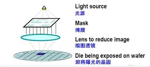
1. Photocopying process: The device or circuit pattern prefabricated on the reticle is accurately transferred to the thin layer of photoresist pre-coated on the wafer surface or dielectric layer according to the required position through the exposure system.
2. Etching process: Use chemical or physical methods to remove the unmasked wafer surface or dielectric layer of the resist thin layer, so as to obtain a pattern completely consistent with the resist thin layer pattern on the wafer surface or dielectric layer. The functional layers of the integrated circuit overlap three-dimensionally, so the photolithography process is always repeated many times. For example, large-scale integrated circuits require about 10 photolithography to complete the transfer of all layers of patterns.
Lithography technology in a narrow sense, lithography process only refers to photocopying process.

Development of lithography technology
In 1947, Bell Labs invented the first point-contact transistor. Since then, lithography technology began to develop.
In 1959, the world's first transistor computer was born, proposing a photolithography process. Fairchild Semiconductor developed the world's first single-structure silicon wafer.
In the 1960s, Xiantong proposed the CMOS IC manufacturing process, the first IC computer IBM360, and established the world's first 2-inch integrated circuit production line. The American GCA company developed an optical pattern generator and a distributed repeating shrinking machine.
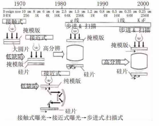
In the 1970s, GCA developed the first distributed repetitive projection exposure machine, and the line width of integrated circuit graphics was reduced from 1.5μm to 0.5μm nodes.
In the 1980s, the United States SVGL company developed the first generation of step-scanning projection exposure machine, integrated circuit graphics line width reduced from 0.5μm to 0.35μm node.
In the 1990s and n1995, Cano embarked on a 300mm wafer exposure machine and launched EX3L and 5L steppers; ASML launched FPA2500, a 193nm wavelength step scanning exposure machine. Optical lithography resolution reaches the "limit" of 70nm.
Since 2000, while optical lithography has strived to break through the resolution "limit", NGL is researching, including extreme ultraviolet lithography, electron beam lithography, X-ray lithography, nanoimprint technology, etc.
Optical lithography
Optical lithography is to draw the structure pattern of the large-scale integrated circuit device on the mask on the silicon wafer coated with photoresist by projection method of Guangde irradiation. Through the irradiation of light, the components of the photoresist chemically react to form Circuit diagram. The minimum size that can be obtained by limiting the finished product is directly related to the resolution that the lithography system can obtain, and reducing the wavelength of the illumination light source is the most effective way to increase the resolution. For this reason, the development of new short-wavelength light source lithography machines has always been a research hotspot in various countries.
In addition, according to the interference characteristics of light, using various wavefront techniques to optimize process parameters is also an important means to improve resolution. These technologies are breakthroughs in the in-depth analysis of exposure imaging using electromagnetic theory combined with photolithography. Among them are phase-shifting masks, off-axis illumination technology, and proximity effect correction. Using these techniques, higher resolution lithographic patterns can be obtained at the current level of technology.
From the 1970s to the 1980s, lithography equipment mainly used ordinary light sources and mercury lamps as exposure light sources, and their feature sizes were above the micron level. Since the 1990s, in order to meet the requirements of the gradual improvement of IC integration, g-line, h-line, I-line light sources and KrF, ArF and other excimer laser light sources have appeared. At present, the development direction of optical lithography technology is mainly to shorten the wavelength of the exposure light source, increase the numerical aperture, and improve the exposure method.
Phase shift mask
The lithography resolution depends on the partial coherence of the illumination system, the spatial frequency and contrast ratio of the mask pattern, and the numerical aperture of the imaging system. The application of phase shift mask technology may use traditional lithography technology and i-line lithography machine under the best illumination to scribe half the size of the traditional method, and has a larger depth of focus and exposure range. The phase shift mask method has the potential to overcome the limitations of traditional lithography methods for line/space patterns.
With the development of phase shift mask technology, many types have emerged, which can be roughly divided into alternating phase shift mask technology and attenuated phase shift mask technology; edge-enhanced phase shift mask, including sub-resolution phase Shift mask and self-aligned phase shift mask; chromium-free fully transparent phase shift mask and composite phase shift method (alternate phase shift + fully transparent phase shift + attenuation phase shift + binary chromium mask). In particular, alternating and fully transparent phase-shifting masks have the most significant improvement in resolution, creating favorable conditions for sub-wavelength lithography.
The characteristic of the fully transparent phase shift mask is that the edge of the transparent phase shifter pattern with a width greater than a certain width suddenly changes by 180 degrees. The interference effect of the diffraction fields on both sides of the phase shifter edge produces a "blade" light intensity distribution. , And form a dark area with zero light intensity on all the boundary lines of the phase shifter, which has the effect of splitting fine lines into two, which improves the imaging resolution by nearly 1 times.
The potential of optical exposure technology, both theoretically and practically, is amazing. Among them, the use of controlling the optical phase parameters in the optical exposure process produces the interference effect of light, which partially cancels out the diffraction effect that limits the resolution of the optical system. The resolution enhancement technology represented by the wave front engineering plays an important role, including: phase shift mask Mode technology, optical proximity effect correction technology, off-axis illumination technology, pupil space filtering technology, standing wave effect correction technology, defocusing superimposed enhanced exposure technology, surface imaging technology and multi-level glue structure process technology. The most noticeable progress in practical use is the phase shift mask technology, optical proximity effect correction technology and off-axis illumination technology, especially the breakthrough in immersion lens exposure technology and the application of double exposure technology for resolution enhancement The application of technology has created favorable conditions.
Electron beam lithography
Electron beam lithography is a key technology for the development of micro-technology processing, and he plays an irreplaceable role in the field of nano-fabrication. Electron beam lithography mainly depicts tiny circuit diagrams, and circuits are usually in nanometer micro-units. The electron beam lithography technology does not require a mask, and directly focuses the focused electron beam spot on the substrate coated with photoresist.
For electron beam lithography to be applied to the processing of nanoscale microstructures and integrated circuit lithography, several key technical issues must be resolved: electron beam high-precision scanning imaging has low exposure efficiency; electrons in resists and substrates Proximity effects caused by scattering and backscattering phenomena; in the process of realizing nano-scale processing, electronic resist and electron beam exposure, development, etching and other technical problems.

Practice has proved that the application of electron beam proximity effect correction technology, electron beam exposure and optical exposure system matching and hybrid lithography technology and resist exposure process optimization technology are a way to improve the actual lithographic resolution of electron beam lithography systems. Effective way. The most important thing in electron beam lithography is metallization. The first step is to scan the pattern on the surface of the photoresist. The second part is to develop the exposed pattern to remove the unexposed part. The third part deposits metal on the formed pattern. The fourth part removes the photoresist. In the process of metal stripping, the key lies in the photolithography process. Glue control. It is best to use thick glue, which is conducive to the penetration of glue, forming a clear morphology.
Focused particle beam lithography
Focused ion beam (Focused Ion beam, FIB) system uses an electric lens to focus the ion beam into a very small size micro-cutting instrument. Her principle is similar to electron beam lithography, but electrons become ions. The ion beam of the current commercial system is a liquid metal ion source, and the metal material is gallium, because gallium has a low melting point, low vapor pressure, and good oxidation resistance; typical ion beam microscopes include liquid metal ion sources and electric lenses , Scanning electrode, secondary particle detector, 5-6 axially moving specimen base, vacuum system, anti-vibration and magnetic field device, electronic control panel, computer and other hard equipment, external electric field applied to liquid metal ions The source can make the liquid gallium form a small tip, and the negative electric field (Extractor) pulls the gallium at the tip, and the gallium ion beam is derived. At a general working voltage, the tip current density is about 1 Angstrom 10-8 Amp/cm2. Lens focusing, through a series of variable aperture (Automatic Variable Aperture, AVA) can determine the size of the ion beam, and then focus on the surface of the test piece twice, using physical collision to achieve the purpose of cutting.
In terms of imaging, the principles of focused ion beam microscopy and scanning electron microscopy are relatively similar, in which the secondary electrons and secondary ions excited by the impact of gallium ion scanning on the surface of the test beam of the ion beam microscope are the source of the image, and the resolution of the image Depends on the size of the ion beam, the acceleration voltage of the charged ions, the strength of the secondary ion signal, the condition of the test piece grounding, and the instrument's anti-vibration and magnetic field conditions. At present, the image resolution of commercial models has reached up to 4nm, although its The resolution is not as good as that of scanning electron microscope and penetrating electron microscope, but for the analysis of fixed-point structure, it does not have the problem of sample preparation and is more economical in working time.
In addition to the extremely high exposure sensitivity and no proximity effect mentioned above, the focused ion beam projection exposure also includes that the depth of focus can be controlled greater than the depth of exposure. The ion beam emitted by the ion source has very good parallelism. The numerical aperture of the ion beam projection lens is only 0.001, and the depth of focus can reach 100 μm. That is to say, any fluctuation of the surface of the silicon wafer is within 100 μm, and the resolution of the ion beam is basically constant. The focal depth of optical exposure is only 1 ~ 2μm. Her main role is to repair the circuit, make abnormal analysis on the production line or perform photoresist cutting.
EUV lithography
In the development process of microelectronics technology, people have been researching and developing new IC manufacturing technology to reduce line width and increase chip capacity. We also commonly refer to soft X-ray projection lithography as extreme ultraviolet projection lithography. In the field of lithography technology, our scientists have made the most in-depth research on extreme ultraviolet projection lithography EUV technology and have made breakthrough progress, making the extreme ultraviolet projection lithography technology most widely used in future integrated circuit production. It supports the production and use of integrated circuits with 22nm and smaller line widths.

EUV is the deepest sub-micron lithography technology that is currently closest to practical use. Excimer laser lithography with a wavelength of 157nm will also be put into use in the near future. If EUV with a wavelength of 13nm is used, a thin strip of 0.1um can be obtained.
Around 1985, predecessors have theoretically discussed EUV technology and made many related experiments. Nearly a decade later, the development of the microelectronics industry has been hampered by obstacles and people have a sense of worry. And from the development process of microelectronic technology, it can be judged that if the extreme ultraviolet lithography technology is not introduced as soon as possible to make comprehensive improvements to the current chip manufacturing method, it will make the entire chip industry in a precarious position.
The EUV system is mainly composed of four parts: an extreme ultraviolet light source; a reflective projection system; a lithography mask; and a photo-resist coating that can be used for extreme ultraviolet.
The lithography machine used by the extreme ultraviolet lithography technology has an alignment precision of 10 nm. The principle of its R&D and manufacturing is actually very similar to that of traditional optical lithography. The research focus of the lithography machine is to require extremely fast and precise positioning and field-by-field leveling and focusing technology, because the lithography machine has many times of stitching patterns and stepping scanning exposure when working. Not only this, the problems of collection and processing of incident alignment light wave signals need to be solved.
Current status of EUV technology
The progress of EUV technology is relatively slow, and it will consume a lot of capital. Although few manufacturers currently apply this technology to production, extreme ultraviolet lithography has been a research hotspot in recent years. All manufacturers are also full of expectations for this technology, hoping that this technology can be more Great progress can be put into large-scale use at an early date.
Every manufacturer knows that the use of EUV technology is a must for semiconductor technology. The shorter the wavelength, the higher the frequency, and the energy of light is proportional to the frequency and inversely proportional to the wavelength. But because the frequency is too high, the traditional photosol is directly penetrated. Now, the development of semiconductor technology has been restricted by many physical disciplines from various aspects.

In the 45nm process etching, EUV technology has shown some characteristics, so now EVU technology needs to break through, from the external support, to change the photosol, but the appropriate has not been found [3]. In terms of EUV technology itself, at the same time try to reduce the output energy as much as possible.
Problems with current EUV lithography technology:
1. The cost is too high, up to 65 million US dollars, which is more expensive than the 193nm ArF immersion lithography machine;
2. No suitable light source is found;
3. There is no defect-free mask;
4. No suitable photoresist has been developed;
5. Lack of human resources;
6. Can be used for early development of 22nm process.
EUV lithography technology prospects
Under the law of Moore's Law and in the information age of rapid development of science and technology, a new generation of lithography technology should be selected and studied. It is the most concerned in the current microelectronics industry. Among these high-tech, extreme ultraviolet light Compared with other technologies, Carve has obvious advantages. The resolution of EUV lithography can be at least below 30nm, and it is easier to be favored by various integrated circuit manufacturers, because EUV lithography is an extension of traditional lithography technology, and integrated circuit designers also prefer to choose this A lithography technology that fully complies with design rules. Extreme ultraviolet lithography technology masks are not difficult to manufacture and have certain yield advantages.
The manufacturing cost of EUV lithography technology equipment is very high, and many aspects including masks and processes cost a lot of money. At the same time, the design and manufacture of the extreme ultraviolet lithography optical system is also extremely complex, and there are many unresolved technical problems, but solutions to these difficult problems are being studied. Once these problems are solved, extreme ultraviolet lithography technology is used in large-scale integrated circuits In the process of production and application, there will be no technical difficulties in principle.
X-ray lithography
In 1895, the German physicist Roentgen first discovered X-rays, and thus won the Nobel Prize in Physics. X-ray is an electromagnetic wave with wave-particle duality like other particles. It can be a transition of heavy atom energy level or a product of accelerated radiation coupling electron and electromagnetic field. The wavelength of X-rays is extremely short. X-rays were first proposed for lithography in 1972. The wavelength of X-rays used for lithography is usually between 0.7 and 0.12 nm. Its strong penetration determines it High-resolution graphics can also be defined on thick materials.
X-ray lithography basic process
The X-ray wavelength is extremely short, so that it will not cause serious diffraction. When we use X-rays for exposure, the choice of wavelength is limited by certain factors. During the exposure process, the photoresist will absorb X-ray photons and produce photoelectrons whose range changes sequentially with the change of X-ray wavelength. These photoelectrons will To reduce the lithography resolution, the shorter the X-ray wavelength, the farther the range of photoelectrons is, and the more disadvantageous it is for lithography. Therefore, increasing the X-ray wavelength helps to improve the lithographic resolution. However, long-wavelength X-rays will widen the line width of the pattern. Considering the influence of various factors, the wavelength of X-rays can usually only be compromised.
Research this year has found that when the line width of the pattern is small to a certain extent (generally below 0.01 μm), it is affected by the waveguide effect, and the resulting line width of the pattern is smaller than the actual mask pattern, so the resolution of X-ray lithography is also affected. The effect of the distance between the reticle and the wafer.
In addition, a lot of experimental research is needed to solve the many factors that affect the quality of graphics during the micromachining of X-ray lithography patterns.

Ray lithography mask
Among the techniques of post-optical lithography, the most important and difficult technique is the mask manufacturing technique, in which 1:1 lithography is very difficult, which is one of the difficulties that hinder the development of the technology. Therefore, we believe that mask development is an important part of its application to industrial development and the key to success or failure. In the past development, scientists have made great progress on it, there are also some new materials discovery and application, some have been practiced in the laboratory, but there is still no major achievement for industrial development.
The basic structure of an X-ray mask includes a thin film, an absorber, a frame, and a substrate. Among them, Si, SiC, and diamond are generally used as the base material of the thin film. The absorber mainly uses gold, tungsten and other materials, and its structural diagram is shown in the figure:

The performance requirements for the mask are as follows:
1. To be able to effectively transmit X-rays and other light, and ensure that it has sufficient mechanical strength, high X-ray absorption, and thick enough.
2. The amount of aspect ratio is guaranteed, and it must have high resolution and contrast.
3. For the size of the mask, the accuracy must be guaranteed, and there should be no defects or fewer defects.
For substrates like Si3N4 films, low-pressure CVD is often used, and evaporative sputtering plating is often used to manufacture absorbers. In order to improve the quality of X-ray masks, it is necessary to select materials and optimize processes.
X-ray lithography not only has high resolution, but also has the advantage of higher yield. According to the current status of the application of X-ray lithography technology, mass production should be put into play to play a more important role in the production of large-scale or ultra-large-scale IC circuits. Breaking through the difficulties of high-precision pattern mask technology is already on the verge.
Nanoimprint lithography
Nanoimprinting technology was first proposed by Zhou Yu, a Chinese scientist at Princeton University in the 20th century in 1995. This technology has the advantages of high production efficiency, low cost, and simple process. It has been proved to be one of the most promising next-generation lithography technologies for nanoscale large-area structure replication. At present, this technology can achieve a level of resolution below 5 nm. Nano-imprint technology mainly includes thermal imprint, ultraviolet imprint and micro-contact printing.
Nanoimprint technology is the most commonly used method for processing polymer structures. It uses high-resolution electron beams and other methods to make complex nanostructure patterns on the stamp, and then uses the pre-patterned stamp to deform the polymer material and polymerize it. The structure pattern is formed on the object.
1. Hot stamping technology
Nano-hot stamping technology is a low-cost and fast method to obtain parallel replication structures at the micro-nano scale. This technology can copy the structure of the seal to a large surface as needed under high temperature conditions, and is widely used in micro-nano structure processing. The entire hot stamping process must be performed in a vacuum environment with an air pressure of less than 1Pa to avoid distortion of the stamping pattern due to the presence of air bubbles. The hot stamping stamp is made of SiC material. This is because SiC is very hard and reduces the stamping. The possibility of breakage or deformation during the process.
In addition, SiC is chemically stable and does not react with most chemicals, so it is easy to clean the seal with different chemicals after the imprinting. In the process of making the seal, first coat a chromium film with a high selectivity (38&1) on the SiC surface, as an etching mask for subsequent process reactive ion etching, and then uniformly apply ZEP anti-corrosion on the chromium film Etching agent, then use electron beam lithography to etch nano patterns on the ZEP resist. In order to break the chemical bond of SiC, a high voltage must be applied to SiC. Finally, at 350V DC voltage, reactive ion etching was used to obtain a nano-pattern with a smooth etched surface and vertical plane on the SiC surface.

The entire hot stamping process can be divided into three steps:
(1) The polymer is heated above its glass transition temperature. This can reduce the viscosity of the polymer during the imprinting process and increase the fluidity. Under certain pressure, it can quickly deform. But too high temperature is not necessary, because it will increase the time of heating and cooling, which will affect the production efficiency, but there is no obvious improvement on the molded structure, or even bend the polymer and cause damage to the mold. At the same time, in order to ensure that the polymer maintains the same viscosity throughout the imprinting process, the heating temperature must be controlled by the heater.
(2) Apply mechanical pressure on the seal, about 500 ~ 1000KPa [9]. Increase the pressure between the seal and the polymer to fill the cavity in the mold.
(3) After the embossing process is completed, the entire laminate is cooled below the glass transition temperature of the polymer to cure the pattern and provide sufficient mechanical strength to facilitate demolding. Then, the residual polymer (PMMA) is removed by reactive ion etching, and the nanopattern on the template is completely transferred to the polymer on the surface of the silicon substrate, and then the pattern is transferred to the silicon substrate in combination with etching technology.
2. Ultraviolet imprint lithography technology
In the UV imprinting process, the monomer-coated substrate and the transparent seal are loaded into the aligning machine, and are fixed on the respective chucks under a vacuum environment. When the optical alignment of the substrate and the seal is completed, contact imprinting begins. UV exposure through the stamp promotes polymerization and curing of the polymer in the imprinted area.
Compared with thermal imprinting technology, UV imprinting has lower environmental requirements, and can be carried out only at room temperature and low pressure, so that the use of this technology can greatly shorten the production cycle and reduce seal wear. Due to the needs of the process, the production of UV embossed seals requires the use of materials that can be penetrated by ultraviolet light.

In the past, the stamp in the UV embossing process was made by coating PDMS material on a quartz substrate. PDMS is an elastic body with a small Young's modulus, and the soft seal made with it can achieve high resolution. However, in the subsequent experiments, it was found that due to the physical softness of PDMS, it is also easy to deform under low external pressure during the imprinting process. Recently, the French National Nanostructure Laboratory proposed the use of a 3-layer structured soft seal , To reduce the deformation of the UV stamp.
The seal uses a 2mm thick quartz substrate, the middle layer is a PDMS buffer layer with a thickness of 5mm, and the top layer is composed of PMMA. The specific step of making the seal is to uniformly coat PMMA on the ion-activated PDMS material, plate a 30nm thick germanium film on the PMMA as an etching mask in the subsequent process, and then coat the germanium film A resist with high electron beam sensitivity, followed by electron beam lithography and reactive ion etching can obtain a high aspect ratio pattern on the top layer of the stamp PMMA, and finally the residual germanium film can be removed. Using this method can greatly improve the rigidity of the seal and reduce the stamping deformation of the seal while maintaining high resolution.
Hybrid IP65 Solar Power Inverter
Shenzhen Jiesai Electric Co.,Ltd , https://www.gootuenergy.com