The working principle of AD831
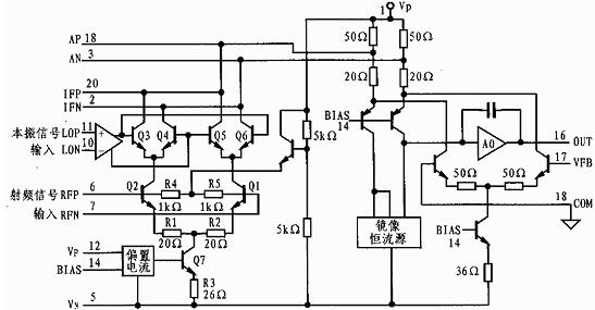
Figure 2 shows the block diagram of the internal circuit of the AD831. In the figure, the frequency input signal is added to the bases of the transistors Q1 and Q2. Due to the negative feedback of the resistors R1 and R2, the amplitude of the differential current RF signal is linear. The -10dBm local oscillator input signal is converted into a square wave through a high-gain, low-noise limiting amplifier, and then cross-connected to the base of Q3 ~ Q6, and finally the mixed signal is output from the IFP and IFN pins. When IFP and IFN are connected to a transformer with a center tap, the AD831 cannot provide a single output from RF to IF. If an output amplifier is used, the IFP and IFN pins can be directly connected to the AP and AN pins. At this time, the on-chip load resistance can convert the output current into a voltage to drive the output amplifier.
2.2 Control bias current
The maximum value of the RF output of the AD831 is proportional to the bias current. Connecting a resistor between the BIAS pin and the power supply can reduce the bias current. In normal operation, the BIAS pin can be left floating, while in low-power operation, the BIAS pin can be directly connected to the positive power supply. The working current of the mixer can be adjusted from 100mA in normal operation to 45mA at minimum power consumption. 2.3 Low-pass filtering
A simple low-pass filter can be added between the mixer and the output amplifier by connecting an external capacitor in parallel with the internal resistive load of the chip (the internal resistive load of the chip is 14Ω, allowing a 20% deviation), This will significantly attenuate the sum frequency component of the local oscillator signal and the RF signal in the downmix application. The corner frequency of the first-order low-pass filter should be selected to be one octave higher than the down-mixed IF output. For example, for the 70MHz IF output, the -3dB point can be selected around 140MHz, and the CF should be 82pF.
2.4 Application of output amplifier
The output amplifier of the AD831 can convert the mixed differential current into a single-ended voltage output, and can provide a peak-to-peak voltage of up to 1V on a 50Ω load. Connect AN and AP directly to the collector output of the mixing stage, and connect the output (OUT) to VFB to provide a single gain. When changing the gain, an external resistor network R3, R4 can be connected to the output of the amplifier and connected to VFB.
3 Application in the local oscillator of frequency-tracking radar
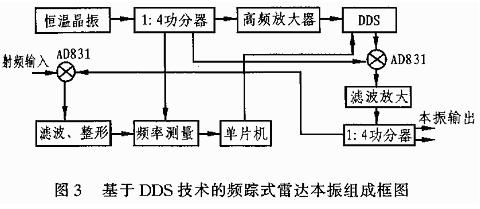
Figure 3 is a block diagram of the local oscillator composition of a frequency-tracking radar based on direct digital frequency synthesis technology (DDS). The system uses two AD831, which are used as down-mix and up-mix.
The 100MHz signal with a frequency stability of 10-9 is generated by a constant temperature crystal oscillator. The power divider is divided into four channels: one channel is amplified and used as the DDS clock; The signal is mixed, and after filtering, the intermediate frequency is amplified and used as the local oscillator signal. The local oscillator signal is also divided into four channels by the four power divider, two of which are used as the local oscillator signal of the radar, one is used for detection, and the other is sent to another AD831 RF signal coupled with the radar transmitter for mixing. The lower intermediate frequency signal output by the AD831 is filtered and sent to the frequency measurement circuit to measure the frequency, so that the single chip microcomputer changes the output frequency of the DDS according to the measurement result to achieve frequency tracking and ensure the stability of the frequency of the radar intermediate frequency signal.
Xinxiang Mina Import & Export Co., Ltd. , https://www.mina-motor.cn