The development of microelectronics and micro-mechanical (MEMS) technology has led to the development of modern sensor design in the direction of miniaturization, intelligence, integration, and micro-low power consumption. MEMS technology breaks through the limitations of traditional sensor design due to technical bottlenecks such as quality, volume, and power consumption, and has a wide range of applications in various measurement fields. With the development of wireless technology, sensor technology and wireless technology are more and more closely integrated. The use of wireless technology to develop signal acquisition wireless transmission module can overcome the drawbacks of wired transmission.
In this paper, the three-axis MEMS inertial sensor LIS331DL and the single-chip wireless transceiver nRF905 are combined to construct an acceleration measurement wireless transmission system to avoid the adverse effects caused by the use of transmission wires and the inconvenience in use. The system is characterized by a combination of a power source, an acceleration sensor, a micro controller, and a radio frequency transceiver. The volume is small and the power consumption is low, and the acceleration in the three-dimensional direction of the moving object can be measured. The designed system device can be easily fixed to a moving object, and is particularly suitable for measuring the acceleration of a moving object in a close complex environment.
1 system composition and working principle
The overall structure of the system is shown in Figure 1. The system is divided into two parts: the main and the slave. The slave is responsible for measuring the acceleration of the moving object and transmitting the measurement data by means of RF transmission; the host is responsible for receiving the data transmitted by the slave, displaying the data in real time, and saving the data result to the PC through the RS 232 serial port for analysis.
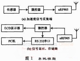
The system is powered by battery and is in standby mode in non-operating mode. The control mode is used to switch between working mode and standby mode to further save power and ensure long-term operation of the battery.
2 hardware design
The hardware design mainly includes the design of the peripheral connection circuit of the sensor and the micro controller, the design of the RF transceiver and the peripheral connection circuit of the micro controller.
2.1 Microcontroller
After comparison, the high-speed C8051F310 single-chip microcomputer is selected as the micro controller of the system. The C8051F310 is a fully integrated mixed-signal system-on-chip MCU chip with a truly independent on-chip system with on-chip power-on reset, VDD monitor, watchdog timer, and clock oscillator.
2.2 LIS331DL sensor circuit design
The LIS331DL is a three-axis linear acceleration sensor with the smallest package (LGA16 package, 3 mm & TImes; 3 mm & TImes; 1 mm) and lowest power consumption (less than 1 mW) in the ST nano motion sensor family.
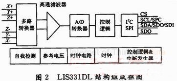
The logic block diagram is shown in Figure 2. The LIS331DL has three sensitive masses placed inside each other. When there is external acceleration, the sensitive mass will deviate from its equilibrium position for a period of displacement, and the larger the external acceleration, the larger the displacement. Since the sensitive mass is located between the capacitances of the two electrodes, the change in the displacement of the mass causes a change in the amount of charge across the capacitor electrode. The change in the amount of charge is converted into a voltage change by the capacitor/voltage converter, A/D conversion. The converter converts the analog voltage value to a binary digital value, which is output in two's complement form from the three output axes of the I2C/SPI serial interface. The chip is capable of measuring the linear acceleration of a moving object in three dimensions, and the vector sum of the accelerations on the three output axes is the acceleration of the moving object.
The chip has a standard I2C/SPI serial bus interface with built-in embedded function, providing users with two programmable ranges of ±2g/±8g for different applications. The data output rate can be programmed to 100 Hz. /400 Hz to accommodate the rate requirements of different peripherals. When the external acceleration value exceeds a programmable acceleration threshold of at least one of the three output shafts, the chip can be configured to generate an inertia wake/free fall interrupt signal. The LIS331DL is able to withstand an acceleration shock of 10 000g while still maintaining its performance.
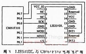
The circuit connection between LIS331DL and C8051F310 is shown in Figure 3. The C8051F310 has a standard SPI serial interface. The four-wire SPI external pin of the C8051F310 (master) is configured by P0.0 (bus clock SCK), P0.1 (master slave MISO), P0. On the four pins of 2 (master-out slave) and P0.3 (slave SPI chip select CS), the LIS331DL acts as the slave of the SPI bus, and the master and slave transmit data through the SPI bus. The bus clock is determined by the host. . The slave's two interrupt flag output pins are connected to the host's P0.6 and P0.7. The crossbar switch in the master configures two external interrupt flag input pins at P0.6 and P0.7, which are connected to the slave. The two interrupt flags of the machine output pins 9 and 11, so that the LIS331DL function can be extended (free fall interrupt detection, internal wake-up, etc.).
2.3 nRF905 microcontroller wireless transceiver circuit design
The nRF905 RF chip is used as the RF transceiver in this measurement system. The nRF905 uses Nordic's VLSI ShockBurst technology. ShockBurst technology enables the nRF905 to provide high-speed data transfer without the need for expensive high-speed MCUs for data processing/clock coverage. By placing high-speed signal processing associated with the RF protocol into the chip, the nRF905 provides an SPI interface to the microcontroller, the rate being determined by the interface rate set by the microcontroller. The nRF905 reduces the average current consumption in the application by reducing the rate of the digital application portion when the RF is connected at the maximum rate through the ShockBurst mode of operation.
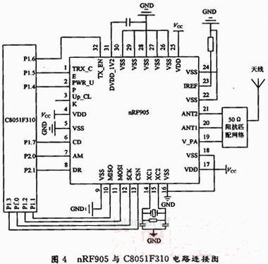
The circuit connection between nRF905 and C8051F310 is shown in Figure 4. The SPI synchronous serial port of C8051F310 has been used as the communication interface with LIS331DL. To make full use of the pin resources of C8051F310, take the four IO ports of P1.0, P1.1, P1.2 and P1.3 of C8051F310 to form an analog SPI. The serial port is connected to the SPI port of the nRF905, and the data is transmitted by single-byte sequential shifting.
The C8051F31O acts as the SPI master and the nRF905 acts as the slave. The host provides the host analog SPI clock on the P1.0 pin, the P1.1 pin as the host analog MISO line, the P1.2 pin as the host analog MOSI line, and the P1.3 pin as the slave SPI chip select line. The host configures the slave related registers in the configuration mode through this analog SPI serial port; transmits and receives the transmitted data in the RF transmit and receive modes. The working status interface of nRF905 is composed of CD, AM and DR; the working mode control pin is composed of PWR, TRX and TX. The C8051F310 sets the working mode of nRF905 through P1.4, P1.5 and P1.6. The specific mode setting is as follows. Table 1 shows.

After entering the ShockBurst RX mode for 650μs, the nRF905 continuously detects and waits to receive data. When the carrier of the same frequency band is detected, the carrier detection pin CD is set high. When a matching address is received, the address detection pin AM is set high. When a correct data packet is received, the nRF905 automatically removes the word. Head, address and CRC check bits, then set the DR pin high to inform the MCU to read the data, and the DR pin is deasserted after the data is read.
When there is data to be sent, the MCU transmits the address of the receiver and the data to be transmitted to the nRF 905 in time series, and the SPI interface rate is determined at the time of communication protocol and device configuration. After entering the Shock Burst TX mode 650us, the RF register is automatically turned on, data packing (plus header and CRC check code), and transmitting data packets. When the data transmission is completed, the DR pin is set high to notify the MCU that the data has been successfully transmitted.
The HP laptop charger is used to recharge the battery in HP notebook and to provide dependable power for operating the notebook for long periods of time. If the original power charger fails, a replacement AC power charger is necessary, and you can buy all kinds of the HP replacement Laptop Charger from YIDASHUN.
HP/Compaq laptop include hp chromebook series, hp pavilion series, hp envy series, hp eliteBook series, hp stream series and so on. Different specifications of laptop charger Adapter is suitable for different laptop model. Such as 90W 19.5V 4.62A with 4.5*3.0 dc tip, it applies for the HP Touchsmart Sleekbook 15 17 M6 M7 Series; HP Pavilion 11 14 15 17, HP Stream 11 13 14 etc. The common HP laptop charger specification has 30W 19V 1.58A, 65W 18.5V 3.5A, 90W 19V 4.74A etc, and the dc tip has common 5.5*2.5mm, 4.8*1.7mm, 7.4*5.0mm and 4.5*3.0mm etc. Also YIDASHUN can produce new usb type c laptop adapter, there are 20W, 45W and 65W.
Yidahsun's laptop adapter are with smart IC to protect your laptop with over current protection, over load protection, short circuit protection and over heat protection!
All Yidashun hp computer charger is Brand New Replacement Product, works as Genuine parts, 100% OEM Compatible!!


HP Laptop Charger,Compaq Laptop Charger,HP Notebook Charger,HP Computer Charger
Shenzhen Yidashun Technology Co., Ltd. , https://www.ydsadapter.com