introduction
All analog-to-digital converters (ADCs) have a certain amount of noise that is converted to the input – it is seen as a noise source model in series with the input of the noise-free ADC. Noise that is reduced to the input cannot be confused with quantization noise, which is only meaningful when the ADC processes signals that change over time. In most cases, the smaller the input noise, the better; but in some cases, the input noise actually helps to improve the resolution. If you don't think this seems to make sense now, then read this article to find out how some noise can be good noise.
Noise converted to the input (code transition noise)
The actual ADC deviates from the ideal ADC in many ways. The noise that is converted to the input (also known as the effective input noise) is undoubtedly deviated from the ideal value, and its effect on the total transfer function of the ADC is shown in Figure 1. As the analog input voltage increases, the "ideal" ADC (shown in Figure 1a) maintains a constant output code until a transition region is reached, at which point the output code immediately transitions to the next quantized value and remains there until Go to the next transition area. The theoretically ideal ADC has zero code transition noise and the width of the transition region is equal to zero. The actual ADC has a certain amount of code transition noise and thus has a limited transition region width. Figure 1b shows the case where the code transition noise width is approximately one least significant bit (LSB) peak-to-peak (PP) noise.
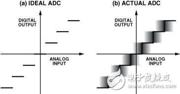
Figure 1. Code transition noise (corresponding to the noise at the input) and its effect on the ADC transfer function
From an internal structure, all ADC circuits generate a certain amount of RMS noise due to resistor noise and "kT/C" noise. This noise, even for DC input signals, appears to be the cause of the code transition noise and is now commonly referred to as noise that is converted to the input. The most common characterization method for noise that is converted to the input is to examine the histogram of a large number of output samples while the input of the ADC is held at a constant DC value. The output of the highest speed or highest resolution ADC is the distribution of the code, usually centered around the DC input nominal value (see Figure 2).
To measure the amount of noise that is converted to the input, ground or connect the input of the ADC to a deeply decoupled voltage source, then acquire a large number of output samples and plot them as a histogram (if the input nominal value of the ADC is 0 V, it is called the input ground histogram). Since the noise is an approximate Gaussian distribution, the standard deviation σ of the histogram can be calculated, which is equivalent to the RMS input noise. For a detailed description of how to calculate the σ value from the histogram data, see in-depth reading 6. The usual practice is to use the RMS of the LSB to represent this RMS noise, which is equivalent to the RMS voltage that is converted into the full-scale input range of the ADC. If the analog input range is expressed in numbers or numbers, the input value (eg, σ) can be expressed in terms of the number of LSBs.
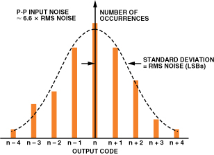
Figure 2. Effect of noise coupled to the input on the input ground histogram of the ADC with a small DNL
Although the inherent differential linearity error (DNL) of the ADC can cause deviations from the ideal Gaussian distribution (for example, some DNLs in Figure 2 are obvious), they should at least approximate the Gaussian distribution. If there is a significant DNL deviation, then the sigma value should be calculated averaged for several different DC input voltages. If the code distribution is obviously non-Gaussian, such as large and obvious peaks or troughs, this indicates that the ADC is not well designed, or it is likely that the printed circuit board (PCB) is not well routed, the grounding technique is poor, or the power supply Decoupling is incorrect (see Figure 3). Another sign of trouble is that the width of the Gaussian distribution changes drastically when the DC input of the ADC exceeds the input voltage range of the ADC.
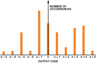
Figure 3. Input ground histogram for poor ADC design and poor PCB layout, grounding, or decoupling
RS232 Wireless Modem is used to replace wired RS232 serial communication cables. PufangTech`s RS232 Wireless Modem can establish a transparent radio serial connection between point to point or among point to multi-point stations in half duplex mode.
The wireless modem has a robust range of 1 to 10Km through buildings and up to 50Km line of sight without any special antenna configurations. It transmits and receives RS232 data at interface baud rates of 1200bps to 115200bps. The low cost unit operates on VHF/UHF frequency band and is modulated with narrow band digital FM.
It can be used in any remote supervision and control applications such as master stations of oil, gas and water pipelines, environmental monitoring, street light control, wastewater pumping stations and OEM applications.
RS232 Wireless Modem
RS232 Wireless Modem,Wireless RS232,RF Modem RS232,RS232 Wireless GSM Modem
Shenzhen PuFang Technology Co., Ltd. , https://www.hytelus.com