Abstract: In the design of flight simulator, in order to enable data to be transmitted quickly and efficiently between modules of flight simulator, a design method using FPGA as the core processor in CAN bus node structure is proposed. The software and hardware design of the flight simulator communication interface is completed. Programming with Verilog HDL enables efficient reading and writing of the SJA1000 bus controller. The actual test shows that compared with the single-chip microcomputer as the processor, the design is scalable, easy to modify and transplant, and can reduce the cost of the simulator.
The flight simulator is a necessary equipment for modern pilot training. It is an analog device that is controlled by a computer in real time, coordinated by multiple systems, and can simulate a real flight environment. Compared with the flight training using aircraft, the simulated flight training using the flight simulator is not only restricted by natural conditions such as weather, but also has no limitations such as logistics, maintenance and flight safety. Many units at home and abroad have developed training simulators of various types and sizes, and achieved good training results, ensuring the successful completion of the mission.
In the design of the flight simulator, a large amount of information is required to be transmitted at high speed between the modules of the flight simulator quickly and efficiently, which requires a certain communication interface protocol to realize data interaction. At present, the flight simulator usually adopts the CAN bus as the communication protocol, and uses the single chip microcomputer as the microprocessor, which has poor expandability. According to the structural characteristics of the flight simulator, the paper analyzes the development of fieldbus technology and FPGA technology. According to the actual needs of the flight simulator and the characteristics of the bus itself, the CAN bus is selected as the communication method between the host and the field device, and the FPGA is used as the communication method. The core processor in the CAN bus node structure is designed for the flight simulator communication interface.
1 hardware system design
The CAN (Controller Area Network) bus is a serial communication bus and is one of the most widely used open field buses in the world. CAN was originally designed as a communication for microcontrollers in automotive environments, but because of its flexibility, reliability, and functionality, it has been widely used in various automatic control fields. The CAN bus has a multi-master structure based on priority and is reliable. Error detection and processing mechanism, high transmission rate (up to 1 Mb/s), long transmission distance (up to 10 km when baud rate is lower than 5 kb/s), which overcomes the low RS-485 network Bus utilization, single master-slave structure, lack of hardware error detection. In the design process of the flight simulator, the main control machine needs to interact with multiple modules, and the CAN bus interface is very suitable.
The hardware design of the flight simulator communication interface uses CAN bus as the communication protocol. ALTERA CYCLONE series EP1C6Q240C8 is selected as the core processor of the CAN node, and the SJA1000T of Philips is used as the CAN bus controller. The CAN bus controller and the CAN physical bus are used. PCA82C250 is selected as the CAN transceiver, in order to enhance the anti-interference ability,
Protect the CAN bus controller and use the 6N137 for optical isolation between the SJA1000T and the PCA82C250 at a speed of 10 MHz. Use Verilog to program the FPGA in the Quartus II software to control the SJA1000T and communicate between CAN nodes. The interface circuit design is shown in Figure 1.

The SJA1000 chip is a stand-alone CAN bus controller. Compared to its previous PCA82C200, the SJA1000 adds the PeliCAN mode to the original BasicCAN mode. This mode supports the CAN2.0B protocol. In order to improve the bus driving capability of SJA1000, PCA82C250 bus transceiver is added between SJA1000 and CAN bus. Its main function is to increase communication distance, improve the instantaneous anti-interference ability of the system, protect the bus, reduce radio frequency interference, realize thermal protection, etc. .
In the system design, FPGA is selected as the core processor of the CAN bus node, which can better adapt to speed and volume, and can enhance the flexibility and scalability of the flight simulator communication interface design, because in the flight simulator design. Sometimes you need to use other communication interfaces, such as RS232 and RS422. EP1C6Q240 is a cost-effective FPGA from ALTERA. It operates at 3.3 V, has a core voltage of 1.5 V, and uses 0.13 μm process technology. It has 5 980 LEs and contains 20 MK4 RAM blocks (128 & TImes; 36 bits). The total RAM space is 92 160 bits, embedded with two phase-locked loop circuits, and the maximum user I/O is 185. The configuration chip selects EPCS1. For the FPGA download mode, JTAG mode and AS mode can usually be used. The way, the hardware connection method is not used. The JTAG method downloads the program to the RAM in the FPGA chip. The program in the FPGA chip cannot be saved after power-off. The JTAG download mode is suitable for debugging the program, and the AS method can download the program to the configuration chip and configure the program in the chip. It can also be saved after power-off, and automatically loaded into the FPGA after power-on and started by the FPGA.
In the CAN bus interface hardware design, it is mainly the interface circuit design between CAN bus controller and FPGA and CAN bus controller and CAN bus transceiver. At design time, FPGA has a rich I/O port compared to the design using a microcontroller as a microprocessor. In order to match the 3.3VI/O interface level of the FPGA with the 5 V TTL level standard of the SJA1000, in the FPGA When connecting with SJA1000, 74ALVC164245 level converter is needed, so AD0~AD7, chip select signals CS, RD, WR, ALE, INT, MODE of CAN bus controller SJA1000 pass through level converter and I/O of FPGA respectively. Connected. In order to enhance the anti-interference ability, the TX output terminal TX0 and the receiving input terminal RX0 of the bus controller SJA1000 are respectively connected to the TXD and RXD of the bus transceiver PCA82C250 via the integrated photocoupler 6N137, and the CANH and CANL ports of the PCA82C250 are directly connected to the CAN physical bus. Connected. The PCA82C250 is the interface between the CAN bus controller and the physical bus. It has the function of differentially transmitting data to and receiving data from the CAN bus controller. In addition, the RX1 pin of the SJA1000 is connected to the VREF pin of the PCA82C250. The input comparator bypass function reduces internal delay and increases the bus length for normal communication.
2 software system design
The software design of the CAN bus node is mainly to program the FPGA. On the one hand, the acquisition and output of various interface data of the flight simulator, on the other hand, the interface logic program of the SJA1000 to control the working mode and working state of the CAN bus. , to send and receive data. Here mainly introduces the programming of the FPGA to the bus controller, mainly including the initialization logic, data transmission logic and data receiving logic of the SJA1000. Since the SJA1000 address bus is multiplexed with the data bus, this requires the FPGA not only to generate the signal logic of the SJA1000 read/write control pin, but also to generate the addressing signal to the SJA1000, which is actually a process of writing an address to the SJA1000. Therefore, the key to the design is to write the register address in the SJA1000 as data to the SJA1000, and at the same time complete the command word write to the SJA1000 specific register with the address latch signal ALE and the write enable signal WR.
2.1 SJA1000 initialization logic
The main function of the initialization logic is to initialize the SJA1000 after the system is powered on or restarted to determine the working frequency, baud rate, output characteristics, and so on. The SJA1000 supports two modes, BasicCAN mode and PeliCAN mode. The BasicCAN mode is the default operation mode after power-on. The initialization logic of SJA1000 mainly includes the setting of working mode, setting of acceptance filtering mode, setting of acceptance mask register (AMR) and acceptance code register (ACH), setting of interrupt enable register (IER), bus timing register (BTR0, BTR1). , output control register (OCR) and clock divider (CDR) settings. After completing the initial setup of the SJA1000, the SJA1000 can be returned to the working state for normal communication tasks.
2.2 Data Transmission Logic
The data transmission logic requires the FPGA to control the SJA1000 through the analog bus method. The register of the SJA1000 transmit buffer has 11 bytes, of which the first 3 bytes are the frame information byte and two identification codes, and the last 8 words. The section is data. When sending, the user needs to combine the data to be sent into a frame message in a specific format, send it to the SJA1000 send buffer, and then start SJA1000 to send. It should be noted that before sending a buffer to the SJA1000, you must first determine whether the send buffer is locked. If it is locked, wait; determine whether the last transmission was completed. If it is not completed, wait for the transmission to complete. The timing diagram of the bus controller write cycle is shown in Figure 2.

2.3 Data Reception Logic
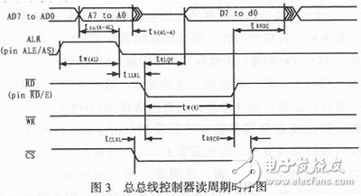
Similar to the data transmission logic, reading a message from the receive buffer also requires 11 bytes to be read continuously. In addition to normal message data reception, the data reception logic needs to be processed in other cases. The CAN receive buffer is released after the data in the receive buffer has been read. Figure 3 shows the timing diagram for the bus controller read cycle.
When the FPGA program is written, the state machine is used to complete the logic design, including initialization state, idle state, query state, data receiving state, and data sending state.
3 Conclusion
In the system design process, ALTERA's EP1C6 FPGA is used for design. Verilog HDL programming is used in the Quartus II environment to generate SJA1000 chip select signals, address latch signals, and read and write signals. These signals together drive the SJA1000 to complete the data. Send and receive. In the process of implementing logic control of SJA1000 by FPGA, the signal of each interface of FPGA is measured by the SignalTap II Logic Analyzer tool in Quartus II. After checking various logics, it meets the interface timing requirements of SJA1000.
The FPGA-based flight simulator communication interface design is mainly described by Verilog language, which is easy to modify and transplant. At the same time, due to the rich I/O of the FPGA, some common switches in the simulator can be connected to the FPGA, so that A variety of functions are integrated on an FPGA. Compared with the single-chip control SJA1000 for CAN bus communication, this design has good scalability, high stability, and can reduce cost, system size and power consumption. It has a field in the field of flight simulators. Wide application prospects.
Salon Trolley Cart,Beauty Trolley Cart,Beauty Salon Cart,Beauty Salon Trolley Cart
TOM SPA BEAUTY SALON EQUIPMENT CO.,LTD , https://www.tomspabeauty.com